NPN and PNP BJTs are bipolar junction transistors that differ primarily in their charge carrier flow, with NPN transistors using electrons as majority carriers and PNP transistors using holes, impacting their switching and amplification properties. Understanding these differences can optimize your circuit design and performance; explore the rest of the article to learn more about their characteristics and applications.
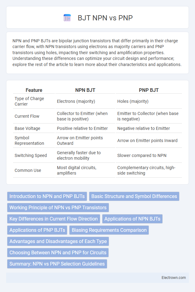
Table of Comparison
| Feature | NPN BJT | PNP BJT |
|---|---|---|
| Type of Charge Carrier | Electrons (majority) | Holes (majority) |
| Current Flow | Collector to Emitter (when base is positive) | Emitter to Collector (when base is negative) |
| Base Voltage | Positive relative to Emitter | Negative relative to Emitter |
| Symbol Representation | Arrow on Emitter points Outward | Arrow on Emitter points Inward |
| Switching Speed | Generally faster due to electron mobility | Slower compared to NPN |
| Common Use | Most digital circuits, amplifiers | Complementary circuits, high-side switching |
Introduction to NPN and PNP BJTs
NPN and PNP BJTs are bipolar junction transistors serving as essential components in electronic circuits for amplification and switching. NPN transistors have electrons as the majority charge carriers, allowing current to flow from the collector to the emitter when a positive voltage is applied to the base. PNP transistors, in contrast, use holes as the majority carriers, conducting current from emitter to collector when the base is at a lower potential than the emitter, making your choice dependent on the specific polarity requirements of your circuit.
Basic Structure and Symbol Differences
NPN and PNP BJTs differ primarily in their semiconductor layer arrangements: NPN transistors have a layer of P-type material sandwiched between two N-type layers, whereas PNP transistors consist of an N-type layer between two P-type layers. The symbols for NPN and PNP BJTs distinguish by the direction of the arrow on the emitter; the NPN symbol arrow points outward, indicating conventional current flow out of the transistor, while the PNP symbol arrow points inward. Understanding these structural and symbolic distinctions helps you accurately interpret circuit diagrams and select the appropriate transistor type for your electronic design.
Working Principle of NPN vs PNP Transistors
NPN and PNP bipolar junction transistors (BJTs) operate based on the movement of charge carriers, with NPN transistors using electron flow from the emitter to the collector through the base, while PNP transistors rely on hole flow from emitter to collector. In an NPN transistor, a small current applied to the base allows a larger current to flow from the collector to the emitter, whereas in PNP transistors, the current flows from the emitter to the collector when a small current leaves the base. Your choice between NPN and PNP transistors depends on the required polarity and application in your electronic circuit design.
Key Differences in Current Flow Direction
In NPN BJTs, current flows from the collector to the emitter when a positive voltage is applied to the base relative to the emitter. PNP transistors, in contrast, conduct current from emitter to collector when the base is at a lower potential than the emitter. Understanding this difference in current flow direction is crucial for designing and troubleshooting your transistor circuits.
Applications of NPN BJTs
NPN BJTs are widely used in switching applications due to their ability to efficiently source current from the positive voltage supply to the load. They dominate amplifier circuits where fast switching and high gain are required, such as in RF amplifiers and digital logic circuits. Power electronics often employ NPN transistors in motor drivers and power regulation circuits because of their superior electron mobility compared to PNP transistors.
Applications of PNP BJTs
PNP BJTs are commonly used in low-side switching applications where the load connects to the positive supply voltage. They serve effectively in amplifier circuits requiring current sourcing and in complementary push-pull configurations for audio amplification. Their ability to conduct when the base is pulled low makes them suitable for controlling high-side loads in specific power management scenarios.
Biasing Requirements Comparison
NPN BJTs require a positive voltage at the base relative to the emitter to forward-bias the base-emitter junction, typically around 0.7V for silicon transistors, ensuring electron flow from emitter to collector. PNP BJTs need a negative voltage at the base relative to the emitter for biasing, with the base voltage approximately 0.7V lower than the emitter to allow hole conduction. The polarity of the power supply and biasing circuits differs between NPN and PNP devices, influencing their integration in circuit designs and requiring careful consideration for proper transistor operation.
Advantages and Disadvantages of Each Type
NPN BJTs offer faster electron mobility, resulting in higher switching speeds and better performance in high-frequency circuits, but they typically require a positive voltage relative to the emitter for operation. PNP BJTs provide easier integration in certain positive ground circuits and offer better performance in low-voltage applications, although they tend to have slower switching speeds and lower current gain compared to NPN types. Your choice depends on circuit requirements, as NPN transistors excel in speed and efficiency while PNP transistors are beneficial for specific polarity and low-voltage uses.
Choosing Between NPN and PNP for Circuits
Choosing between NPN and PNP BJTs depends on the voltage polarity and current direction in your circuit design. NPN transistors are generally preferred for switching and amplification when the load is connected to the positive voltage rail, offering higher electron mobility and faster switching speeds. PNP transistors are suitable for circuits where the load is connected to the ground or negative voltage, allowing for easier sourcing of current in negative polarity scenarios.
Summary: NPN vs PNP Selection Guidelines
NPN transistors are preferred in applications requiring high-speed switching and higher electron mobility due to their majority carrier being electrons, making them efficient for low-side switching. PNP transistors are typically chosen for high-side switching in positive voltage circuits, where current flows from the emitter to the collector, leveraging hole mobility as the majority carrier. Selecting between NPN and PNP BJTs depends on circuit topology, voltage polarity, and switching speed requirements.
NPN vs PNP BJT Infographic