Wet etching uses liquid chemicals to remove material from a surface, offering simplicity and selectivity but limited precision, whereas dry etching employs plasma or reactive gases for more controlled and anisotropic material removal suitable for complex patterns. Explore the rest of the article to understand which etching method best fits your semiconductor or microfabrication needs.
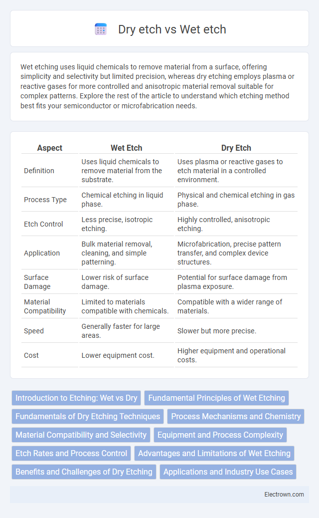
Table of Comparison
| Aspect | Wet Etch | Dry Etch |
|---|---|---|
| Definition | Uses liquid chemicals to remove material from the substrate. | Uses plasma or reactive gases to etch material in a controlled environment. |
| Process Type | Chemical etching in liquid phase. | Physical and chemical etching in gas phase. |
| Etch Control | Less precise, isotropic etching. | Highly controlled, anisotropic etching. |
| Application | Bulk material removal, cleaning, and simple patterning. | Microfabrication, precise pattern transfer, and complex device structures. |
| Surface Damage | Lower risk of surface damage. | Potential for surface damage from plasma exposure. |
| Material Compatibility | Limited to materials compatible with chemicals. | Compatible with a wider range of materials. |
| Speed | Generally faster for large areas. | Slower but more precise. |
| Cost | Lower equipment cost. | Higher equipment and operational costs. |
Introduction to Etching: Wet vs Dry
Wet etching utilizes liquid chemical solutions to selectively remove materials from a substrate through isotropic or anisotropic reactions, making it ideal for applications requiring smooth surface finishes and lower equipment costs. Dry etching employs plasma or reactive gases to precisely etch materials with high anisotropy, enabling fine patterning for advanced semiconductor fabrication and microelectromechanical systems (MEMS). Differences in etch rate, selectivity, and feature resolution between wet etch and dry etch processes influence their choice in industries such as integrated circuit manufacturing and nanofabrication.
Fundamental Principles of Wet Etching
Wet etching relies on liquid chemical solutions to selectively remove materials from a substrate, utilizing isotropic or anisotropic etching mechanisms based on the etchant composition and substrate crystallography. The process efficiently dissolves exposed layers through chemical reactions, making it suitable for uniform material removal with relatively low equipment complexity. Your choice of wet etchant directly influences etch rate, selectivity, and surface morphology, impacting overall device fabrication quality.
Fundamentals of Dry Etching Techniques
Dry etching techniques utilize plasma or reactive ions to selectively remove material from a substrate, offering precise control over etch profiles and anisotropy compared to wet etching. Key dry etching methods include reactive ion etching (RIE), deep reactive ion etching (DRIE), and plasma etching, each exploiting different plasma chemistries and ion energies to achieve specific etch rates and selectivities. Dry etching enables high-resolution pattern transfer in semiconductor fabrication, critical for advanced microelectronic and MEMS device manufacturing.
Process Mechanisms and Chemistry
Wet etch utilizes liquid chemical solutions that selectively dissolve target materials through isotropic reactions, often involving acids like hydrofluoric acid for silicon dioxide. Dry etch employs plasma or reactive gases to remove materials via anisotropic physical sputtering and chemical reactions, enabling precise pattern transfer with enhanced directionality. Understanding these fundamental process mechanisms and chemistry allows you to optimize etching for specific semiconductor fabrication applications, balancing factors like etch rate, selectivity, and feature resolution.
Material Compatibility and Selectivity
Wet etch processes excel in material compatibility by effectively etching a wide range of materials, including metals and oxides, with high selectivity due to the chemical solutions targeted for specific layers. Dry etch offers superior precision and anisotropy, enabling you to achieve detailed pattern transfer with high selectivity by using plasma conditions tailored to react preferentially with certain materials. Choosing between wet and dry etching depends on your process requirements for material type, etch profile, and selectivity in semiconductor fabrication.
Equipment and Process Complexity
Wet etch utilizes chemical baths and simple equipment, making it less complex and more cost-effective for large-scale material removal. Dry etch employs plasma reactors or reactive ion etching systems, requiring advanced equipment and greater control over process parameters, resulting in higher process complexity. The precise anisotropic etching capability of dry etch contrasts with the isotropic nature of wet etch, influencing equipment choice based on device specifications.
Etch Rates and Process Control
Wet etch processes typically exhibit higher etch rates due to chemical reactions in liquid solutions, enabling faster material removal but with less precise process control and potential undercutting. Dry etch techniques, such as plasma or reactive ion etching, offer superior process control through adjustable parameters like gas composition, pressure, and power, allowing for anisotropic etching and finer feature definition. Precise control of etch rates in dry etching translates to better reproducibility and uniformity, critical for advanced semiconductor fabrication.
Advantages and Limitations of Wet Etching
Wet etching offers advantages such as simplicity, low cost, and high selectivity due to its chemical-based material removal processes, making it ideal for bulk etching and isotropic profiles. However, its limitations include less precision, difficulty in controlling etch depth, and potential undercutting, which impacts fine-feature fabrication and pattern fidelity. Your choice between wet and dry etching depends on the required accuracy and application-specific material compatibility.
Benefits and Challenges of Dry Etching
Dry etching offers precise anisotropic profiles and superior control over etch depth, making it ideal for high-resolution semiconductor fabrication. It minimizes undercutting and contamination since it uses plasma or reactive gases instead of liquid chemicals. Challenges include equipment complexity, higher costs, and potential plasma-induced damage to sensitive substrates requiring careful process optimization.
Applications and Industry Use Cases
Wet etch processes are widely used in semiconductor fabrication for cleaning and pattern transfer in applications such as MEMS device manufacturing and wafer thinning, where isotropic etching is sufficient. Dry etch techniques dominate in advanced semiconductor device fabrication, enabling precise anisotropic patterning critical for creating high-aspect-ratio features in integrated circuits and microelectromechanical systems. Industries such as microelectronics, photovoltaics, and MEMS rely on dry etching for its superior control and reproducibility in producing complex nanoscale structures.
Wet etch vs Dry etch Infographic