Junction isolation uses reverse-biased p-n junctions to electrically separate components on a semiconductor chip, providing effective isolation with minimal area consumption, while oxide isolation employs silicon dioxide layers to insulate devices, offering superior dielectric properties but often requiring more complex fabrication. Discover the key differences and benefits of each technique to understand which isolation method best suits your semiconductor design needs.
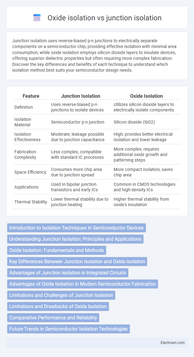
Table of Comparison
| Feature | Junction Isolation | Oxide Isolation |
|---|---|---|
| Definition | Uses reverse-biased p-n junctions to isolate devices | Utilizes silicon dioxide layers to electrically isolate components |
| Isolation Material | Semiconductor p-n junction | Silicon dioxide (SiO2) |
| Isolation Effectiveness | Moderate; leakage possible due to junction capacitance | High; provides better electrical isolation and lower leakage |
| Fabrication Complexity | Less complex, compatible with standard IC processes | More complex; requires additional oxide growth and patterning steps |
| Space Efficiency | Consumes more chip area due to junction spread | More compact isolation, saves chip area |
| Applications | Used in bipolar junction transistors and early ICs | Common in CMOS technologies and high-density ICs |
| Thermal Stability | Lower thermal stability due to junction heating | Higher thermal stability from oxide's insulation |
Introduction to Isolation Techniques in Semiconductor Devices
Junction isolation employs reverse-biased p-n junctions to electrically separate device regions, offering efficient isolation in integrated circuits by preventing current leakage between components. Oxide isolation uses thermal silicon dioxide layers grown on the wafer surface to create insulating barriers, providing superior surface passivation and high resistance to electrical conduction. Both techniques are fundamental in semiconductor device fabrication, influencing device performance, density, and manufacturing complexity.
Understanding Junction Isolation: Principles and Applications
Junction isolation uses reverse-biased p-n junctions to electrically separate devices on a semiconductor chip, preventing current leakage and crosstalk between components. This technique is widely applied in integrated circuits to enhance device reliability and performance by creating effective isolation barriers without needing thick oxide layers. Understanding your design requirements helps determine when junction isolation is preferable over oxide isolation for optimizing semiconductor device functionality.
Oxide Isolation: Fundamentals and Methods
Oxide isolation relies on silicon dioxide layers to electrically separate devices on a semiconductor wafer, preventing electrical crosstalk and leakage currents. Common methods include LOCOS (Local Oxidation of Silicon), which grows thick oxide regions through selective oxidation, and STI (Shallow Trench Isolation), where trenches etched into the silicon are filled with oxide to achieve isolation. These oxide isolation techniques offer superior scalability and reduced parasitic capacitance compared to junction isolation, making them essential for modern integrated circuit fabrication.
Key Differences Between Junction Isolation and Oxide Isolation
Junction isolation uses reverse-biased p-n junctions to electrically separate devices on a semiconductor wafer, providing effective isolation with relatively low parasitic capacitance. Oxide isolation employs thick silicon dioxide layers created through processes like LOCOS or trench isolation, offering superior surface passivation and minimized leakage currents. Key differences lie in oxide isolation's enhanced electrical isolation and reduced surface state density compared to junction isolation's reliance on doped junctions and susceptibility to latch-up.
Advantages of Junction Isolation in Integrated Circuits
Junction isolation in integrated circuits offers superior electrical isolation by using reverse-biased p-n junctions, which reduces parasitic capacitance and leakage currents compared to oxide isolation. It enables higher packing density and improved reliability due to its inherent robustness against contamination and mechanical stress. This method also supports higher voltage operation and better thermal stability, making it advantageous for mixed-signal and high-power IC applications.
Advantages of Oxide Isolation in Modern Semiconductor Fabrication
Oxide isolation offers superior electrical insulation and reduced parasitic capacitance compared to junction isolation, enhancing device performance and reliability in modern semiconductor fabrication. Its compatibility with high-density integration enables smaller component sizes and improved thermal stability, crucial for advanced integrated circuits. You benefit from better scalability and process simplicity, making oxide isolation the preferred choice for contemporary microelectronics.
Limitations and Challenges of Junction Isolation
Junction isolation faces limitations such as increased leakage currents due to minority carrier injection and complex process control needed to form precise p-n junctions. Your device may experience reduced isolation effectiveness at high frequencies because junction capacitance can degrade signal integrity. Thermal budget constraints and doping profile variations also challenge junction isolation, making oxide isolation a more robust alternative in many applications.
Limitations and Drawbacks of Oxide Isolation
Oxide isolation, while effective for electrical separation in integrated circuits, faces limitations such as increased stress-induced defects leading to reliability concerns and higher fabrication complexity due to thermal budget constraints. The silicon dioxide layer may introduce interface states that degrade device performance and cause leakage currents, impacting overall circuit efficiency. Your choice between junction and oxide isolation should consider these drawbacks, especially in high-density or high-performance semiconductor applications.
Comparative Performance and Reliability
Junction isolation offers superior electrical performance with lower parasitic capacitance and better high-frequency operation, making it ideal for high-speed integrated circuits. Oxide isolation provides enhanced reliability through excellent electrical insulation and reduced leakage currents, ensuring stable long-term device operation in harsh environments. Your choice between junction and oxide isolation depends on balancing the need for speed and signal integrity against the requirement for robust, reliable insulation.
Future Trends in Semiconductor Isolation Technologies
Junction isolation and oxide isolation have been foundational in semiconductor device fabrication, but emerging trends favor advanced dielectric materials and trench isolation techniques to enhance device scaling and reduce parasitic leakage. Future semiconductor isolation technologies focus on integrating high-k dielectrics and innovative 3D isolation structures to improve electrical performance and thermal stability while minimizing footprint. Research also emphasizes monolithic integration with heterogeneous materials, optimizing isolation for next-generation FinFETs and gate-all-around (GAA) transistors in nanoelectronics.
Junction isolation vs oxide isolation Infographic