P-well and N-well regions are integral to CMOS technology, with P-wells housing NMOS transistors and N-wells containing PMOS transistors, enabling complementary operation in integrated circuits. Understanding the differences in doping types, electrical properties, and fabrication processes between P-well and N-well is crucial for optimizing your semiconductor device performance; explore the rest of the article to learn more.
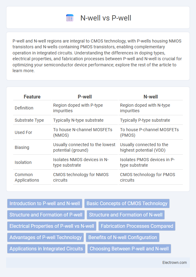
Table of Comparison
| Feature | P-well | N-well |
|---|---|---|
| Definition | Region doped with P-type impurities | Region doped with N-type impurities |
| Substrate Type | Typically N-type substrate | Typically P-type substrate |
| Used For | To house N-channel MOSFETs (NMOS) | To house P-channel MOSFETs (PMOS) |
| Biasing | Usually connected to the lowest potential (ground) | Usually connected to the highest potential (VDD) |
| Isolation | Isolates NMOS devices in N-type substrate | Isolates PMOS devices in P-type substrate |
| Common Applications | CMOS technology for NMOS circuits | CMOS technology for PMOS circuits |
Introduction to P-well and N-well
P-well and N-well are fundamental regions used in CMOS (Complementary Metal-Oxide-Semiconductor) technology to create p-type and n-type transistors respectively. The P-well is a p-type doped region embedded in an n-type substrate, designed to house n-channel MOSFET (NMOS) devices. Conversely, the N-well is an n-type doped region within a p-type substrate, serving as the location for p-channel MOSFET (PMOS) devices, enabling complementary transistor pairs essential for low-power digital circuits.
Basic Concepts of CMOS Technology
P-well and N-well are fundamental structures in CMOS technology used to create complementary MOSFETs by implanting dopants into the silicon substrate; the P-well contains NMOS transistors with n-type channels, while the N-well houses PMOS transistors with p-type channels. These wells provide isolation and help establish the necessary electrical characteristics for high-performance and low-power integrated circuits. Understanding the differences between P-well and N-well is crucial for optimizing your CMOS device designs and ensuring efficient operation in various semiconductor applications.
Structure and Formation of P-well
The P-well is formed by implanting or diffusing acceptor impurities such as boron into an N-type substrate, creating a localized P-type region within the semiconductor. This structure allows for the isolation and incorporation of NMOS transistors in CMOS technology by providing a suitable P-type foundation. The formation process involves controlled doping concentration and thermal diffusion to achieve the desired depth and doping profile for optimal device performance.
Structure and Formation of N-well
The N-well structure is formed by diffusing donor impurities, such as phosphorus or arsenic, into a p-type silicon substrate, creating a region rich in electrons. This well serves as the background for PMOS transistors in CMOS technology, providing the necessary electrical isolation and functionality. Your circuit's performance depends on precise control of the N-well's depth and doping concentration to optimize parameters like threshold voltage and leakage current.
Electrical Properties of P-well vs N-well
P-well regions typically exhibit a positive charge carrier concentration dominated by holes, making them suitable for embedding NMOS transistors with lower substrate leakage currents and improved threshold voltage stability. N-well regions are characterized by a higher concentration of electrons, ideal for housing PMOS transistors and providing better isolation from the P-substrate in CMOS technology. The differing doping types lead to distinct electrical properties such as varying junction capacitances, breakdown voltages, and carrier mobilities, directly impacting device performance and power consumption.
Fabrication Processes Compared
P-well fabrication involves implanting p-type dopants, such as boron, into the silicon substrate to create regions where NMOS transistors reside, while N-well fabrication requires n-type dopants, like phosphorus or arsenic, to form areas for PMOS transistors. The choice between P-well and N-well processes impacts threshold voltage control, isolation techniques, and latch-up susceptibility, with twin-well processes combining both to optimize device performance. Fabrication complexity and cost vary, as N-well processes often demand additional masking and implantation steps compared to single P-well methods.
Advantages of P-well Technology
P-well technology offers superior isolation for NMOS transistors, reducing leakage currents and improving device performance in mixed-signal and analog circuits. It provides better control over threshold voltage variations and enhances immunity to latch-up effects compared to N-well processes. The P-well approach is also favored for its compatibility with low-voltage operation and high-density integration in CMOS fabrication.
Benefits of N-well Configuration
N-well configuration enables the integration of both NMOS and PMOS transistors on the same substrate, facilitating the creation of CMOS technology with improved power efficiency and switching speed. It offers enhanced isolation and reduced latch-up susceptibility by providing a well-defined p-type region for NMOS placement. The N-well structure supports higher voltage tolerance and better noise immunity, making it ideal for mixed-signal and high-performance integrated circuits.
Applications in Integrated Circuits
P-well and N-well regions play critical roles in complementary metal-oxide-semiconductor (CMOS) technology, enabling the integration of both NMOS and PMOS transistors on the same silicon substrate. N-wells are primarily used to house PMOS transistors, while P-wells accommodate NMOS transistors, facilitating efficient low-power and high-speed digital circuits. Your integrated circuit designs leverage the electrical isolation and threshold voltage control offered by these wells to optimize device performance in microprocessors, memory chips, and analog ICs.
Choosing Between P-well and N-well
Choosing between P-well and N-well depends on the type of CMOS technology and device architecture you require; P-wells are typically used for housing NMOS transistors in a P-type substrate, while N-wells accommodate PMOS transistors within an N-type substrate. Your decision should consider factors like latch-up susceptibility, threshold voltage control, and process compatibility, as P-wells offer better isolation for NMOS, whereas N-wells are essential for PMOS integration. Optimizing well selection enhances device performance, reliability, and overall semiconductor process efficiency.
P-well vs N-well Infographic