PMOS transistors conduct when their gate voltage is low, making them ideal for pulling output levels high, while NMOS transistors conduct when their gate voltage is high, efficiently pulling outputs low. Understanding how PMOS and NMOS devices function together in logic gates is essential for optimizing your circuit design, so continue reading to explore their complementary characteristics in depth.
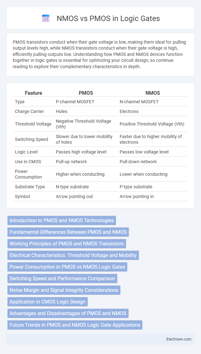
Table of Comparison
| Feature | PMOS | NMOS |
|---|---|---|
| Type | P-channel MOSFET | N-channel MOSFET |
| Charge Carrier | Holes | Electrons |
| Threshold Voltage | Negative Threshold Voltage (Vth) | Positive Threshold Voltage (Vth) |
| Switching Speed | Slower due to lower mobility of holes | Faster due to higher mobility of electrons |
| Logic Level | Passes high voltage level | Passes low voltage level |
| Use in CMOS | Pull-up network | Pull-down network |
| Power Consumption | Higher when conducting | Lower when conducting |
| Substrate Type | N-type substrate | P-type substrate |
| Symbol | Arrow pointing out | Arrow pointing in |
Introduction to PMOS and NMOS Technologies
PMOS and NMOS refer to types of metal-oxide-semiconductor field-effect transistors (MOSFETs), which serve as fundamental building blocks in digital logic design. NMOS transistors conduct when a positive voltage is applied to the gate and offer faster switching speeds with lower electron mobility resistance, making them efficient for pull-down networks. PMOS transistors conduct with a negative gate voltage and are typically used in pull-up networks due to their greater hole mobility, despite slower switching speeds compared to NMOS devices.
Fundamental Differences Between PMOS and NMOS
PMOS transistors use p-type semiconductor material and conduct when the gate voltage is low, while NMOS transistors use n-type material and conduct when the gate voltage is high. NMOS devices typically offer faster switching speeds and higher electron mobility compared to the hole mobility in PMOS devices, impacting overall circuit performance. The complementary use of PMOS and NMOS transistors in CMOS technology leverages these fundamental differences to achieve low power consumption and high noise margins in logic gates.
Working Principles of PMOS and NMOS Transistors
PMOS transistors operate by creating a conductive channel when a low voltage is applied to the gate, allowing current to flow from source to drain via holes as majority carriers. NMOS transistors function by forming a conductive channel when a high voltage is applied to the gate, enabling electron flow from source to drain as majority carriers. The complementary operation of PMOS and NMOS transistors in CMOS logic gates results in low static power consumption and high noise margins, optimizing digital circuit performance.
Electrical Characteristics: Threshold Voltage and Mobility
PMOS transistors have a higher threshold voltage (|Vth| typically around 0.7V) compared to NMOS transistors (|Vth| around 0.3-0.5V), affecting their switching speed and power consumption in logic gates. Electron mobility in NMOS devices (~600 cm2/V*s) is significantly greater than hole mobility in PMOS devices (~250 cm2/V*s), resulting in higher drive current and faster operation for NMOS transistors. These electrical characteristics influence the design of CMOS logic gates, balancing the complementary action to achieve low power dissipation and improved switching performance.
Power Consumption in PMOS vs NMOS Logic Gates
PMOS transistors typically consume less static power than NMOS transistors due to their lower leakage current when in the off state. NMOS logic gates exhibit higher electron mobility, resulting in faster switching speeds but increased dynamic power consumption compared to PMOS devices. Overall, the power efficiency of PMOS logic gates is advantageous in low-power applications, whereas NMOS devices are preferred for high-performance circuits requiring rapid transitions.
Switching Speed and Performance Comparison
PMOS transistors typically have lower electron mobility than NMOS, resulting in slower switching speeds and reduced overall performance in logic gates. NMOS devices provide faster switching due to higher electron mobility, making them preferable in high-speed digital circuits. Your circuit's speed performance can be optimized by leveraging NMOS for pull-down networks and PMOS for pull-up configurations to balance switching efficiency and power consumption.
Noise Margin and Signal Integrity Considerations
PMOS transistors typically exhibit higher noise margins in logic gates due to their stronger pull-up capability and lower threshold voltage variability compared to NMOS devices. NMOS transistors offer faster switching speeds but are more susceptible to signal degradation and reduced noise margins, impacting overall signal integrity. Optimizing logic gate design requires balancing the noise margins and signal integrity properties of PMOS and NMOS to minimize delay and power consumption while maximizing reliability.
Application in CMOS Logic Design
PMOS and NMOS transistors work together in CMOS logic design to create efficient, low-power digital circuits by complementing each other's conductivity characteristics. NMOS devices pull the output low by connecting to ground when activated, while PMOS devices pull the output high by connecting to the supply voltage, enabling robust switching behavior. Your CMOS logic gates benefit from this complementary action, resulting in reduced power consumption and improved performance compared to single-transistor logic families.
Advantages and Disadvantages of PMOS and NMOS
PMOS transistors offer lower electrical noise and better performance in high-voltage applications but suffer from slower switching speeds and larger size compared to NMOS devices. NMOS transistors provide faster switching speeds and higher electron mobility, enhancing overall logic gate performance, yet they typically consume more power due to higher leakage currents. Both transistor types play critical roles in CMOS technology, where complementary pairing mitigates individual disadvantages, optimizing power efficiency and switching speed.
Future Trends in PMOS and NMOS Logic Gate Applications
Future trends in PMOS and NMOS logic gate applications emphasize the integration of advanced CMOS technologies to enhance power efficiency and switching speed. Emerging materials like high-k dielectrics and 2D semiconductors are poised to improve device scalability and reduce leakage currents in both PMOS and NMOS transistors. Research in complementary logic circuits focuses on optimizing threshold voltages and channel lengths to enable ultra-low power consumption in next-generation IoT and wearable devices.
PMOS vs NMOS in logic gates Infographic