Bulk CMOS technology relies on planar transistors with larger leakage currents and lower performance at smaller nodes, while FinFET architecture uses 3D gate structures to improve control over the channel, reducing power consumption and enhancing speed. Explore the rest of the article to understand how these differences impact your device's efficiency and scalability.
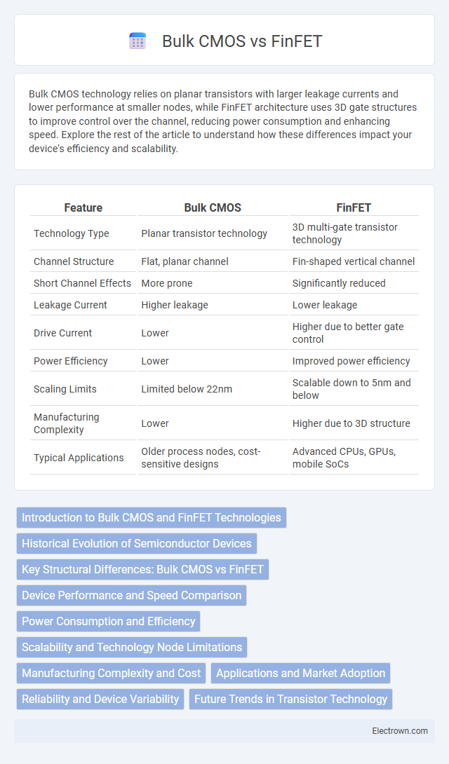
Table of Comparison
| Feature | Bulk CMOS | FinFET |
|---|---|---|
| Technology Type | Planar transistor technology | 3D multi-gate transistor technology |
| Channel Structure | Flat, planar channel | Fin-shaped vertical channel |
| Short Channel Effects | More prone | Significantly reduced |
| Leakage Current | Higher leakage | Lower leakage |
| Drive Current | Lower | Higher due to better gate control |
| Power Efficiency | Lower | Improved power efficiency |
| Scaling Limits | Limited below 22nm | Scalable down to 5nm and below |
| Manufacturing Complexity | Lower | Higher due to 3D structure |
| Typical Applications | Older process nodes, cost-sensitive designs | Advanced CPUs, GPUs, mobile SoCs |
Introduction to Bulk CMOS and FinFET Technologies
Bulk CMOS technology relies on planar transistors fabricated on a bulk silicon substrate, offering simplicity and cost-efficiency for traditional semiconductor manufacturing. FinFET technology, characterized by its three-dimensional fin-shaped channel structure, provides enhanced control over short-channel effects, resulting in improved performance and reduced power consumption. Your choice between Bulk CMOS and FinFET depends on application requirements, with FinFET preferred for advanced nodes and Bulk CMOS still prevalent in mature technology nodes.
Historical Evolution of Semiconductor Devices
Bulk CMOS technology, dominating the semiconductor industry since the 1980s, enabled continuous scaling down of transistor sizes following Moore's Law but faced increasing short-channel effects and leakage currents at sub-20nm nodes. FinFET technology emerged in the early 2010s as a 3D transistor architecture, providing superior control over channel electrostatics and significantly reducing leakage current, which addressed the limitations of planar Bulk CMOS at advanced process nodes. The transition from Bulk CMOS to FinFET marked a pivotal shift in semiconductor device design, catalyzing improved performance, energy efficiency, and scalability in modern integrated circuits.
Key Structural Differences: Bulk CMOS vs FinFET
Bulk CMOS features a planar structure with transistors built on a uniform silicon substrate, whereas FinFET employs a three-dimensional fin-shaped channel that rises above the substrate, enabling better gate control. The multi-gate design of FinFET wraps around the fin, reducing leakage current and improving performance compared to the single-gate Bulk CMOS. Your choice between Bulk CMOS and FinFET depends on the need for power efficiency, scaling, and performance in advanced semiconductor technologies.
Device Performance and Speed Comparison
FinFET technology offers superior device performance and speed compared to Bulk CMOS due to its three-dimensional gate structure, which enhances electrostatic control and reduces short-channel effects. This results in higher drive current and lower leakage power, enabling faster switching speeds and improved energy efficiency in advanced semiconductor nodes. Consequently, FinFET devices dominate in high-performance applications requiring enhanced scalability and speed at sub-20nm technology nodes.
Power Consumption and Efficiency
FinFET technology significantly reduces power consumption compared to Bulk CMOS by minimizing leakage currents through its three-dimensional gate structure, enabling more efficient switching at lower voltages. Bulk CMOS devices exhibit higher static power dissipation due to increased subthreshold leakage, which limits their suitability for ultra-low-power applications. Your choice between these technologies impacts overall energy efficiency, particularly in high-performance and battery-sensitive devices.
Scalability and Technology Node Limitations
Bulk CMOS faces significant scalability challenges as technology nodes shrink below 10nm, encountering increased leakage currents and short-channel effects that degrade device performance. FinFET technology, with its three-dimensional gate structure, offers superior electrostatic control, enabling reliable operation at advanced nodes such as 7nm and 5nm with reduced power consumption. The FinFET architecture addresses the physical limitations inherent in Bulk CMOS, extending Moore's Law by enhancing transistor density and mitigating variability issues at sub-10nm scales.
Manufacturing Complexity and Cost
Bulk CMOS technology offers lower manufacturing complexity and reduced fabrication costs due to its established, planar process, making it cost-effective for high-volume production. FinFET devices require advanced 3D fabrication techniques with precise fin patterning and complex doping profiles, significantly increasing manufacturing complexity and expenses. Your choice between Bulk CMOS and FinFET should consider the trade-off between cost efficiency and improved performance benefits offered by FinFETs.
Applications and Market Adoption
Bulk CMOS technology remains prevalent in low-cost, high-volume applications such as microcontrollers, sensors, and analog circuits due to its mature fabrication process and lower manufacturing costs. FinFETs dominate high-performance and power-sensitive markets, including advanced processors for smartphones, data centers, and AI accelerators, benefiting from superior electrostatic control and reduced leakage currents. The semiconductor industry is rapidly shifting towards FinFET architecture at technology nodes below 10nm, driven by market demand for increased transistor density and energy efficiency.
Reliability and Device Variability
Bulk CMOS technology exhibits higher susceptibility to device variability due to greater random dopant fluctuations and increased short-channel effects impacting reliability. FinFET architecture improves reliability by providing better electrostatic control, reducing leakage currents, and mitigating variability caused by process variations. Enhanced gate control in FinFET devices results in more consistent threshold voltages and improved long-term operational stability compared to Bulk CMOS.
Future Trends in Transistor Technology
Future trends in transistor technology highlight a gradual transition from Bulk CMOS to FinFET architectures as device scaling approaches physical limitations. FinFETs offer superior electrostatic control, reduced short-channel effects, and lower power consumption, making them essential for sub-7nm node advancements. Emerging research focuses on gate-all-around (GAA) transistors and nanosheet FETs to further enhance performance and energy efficiency beyond FinFET capabilities.
Bulk CMOS vs FinFET Infographic