Junction isolation uses reverse-biased PN junctions to electrically separate devices on a semiconductor chip, reducing leakage currents and enhancing device performance, while dielectric isolation employs insulating materials such as silicon dioxide to physically and electrically isolate components, offering superior isolation but at higher manufacturing complexity. Understanding these differences will help you determine the best isolation method for your specific semiconductor applications--read on to explore their mechanisms, advantages, and use cases in detail.
Table of Comparison
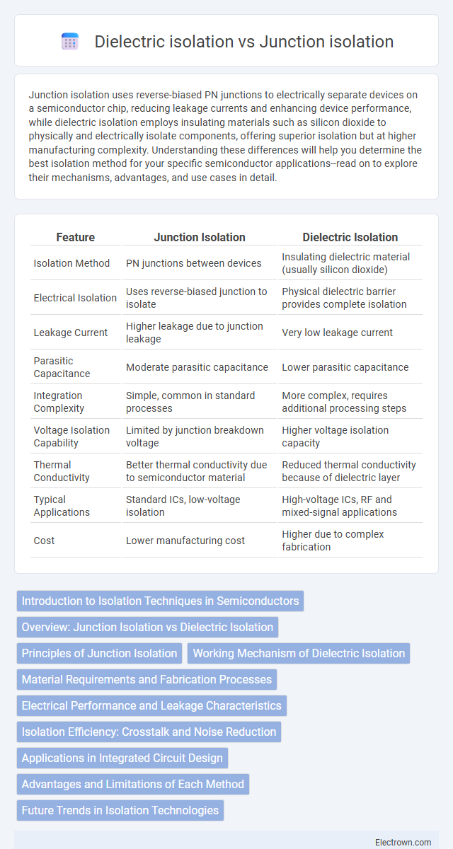
| Feature | Junction Isolation | Dielectric Isolation |
|---|---|---|
| Isolation Method | PN junctions between devices | Insulating dielectric material (usually silicon dioxide) |
| Electrical Isolation | Uses reverse-biased junction to isolate | Physical dielectric barrier provides complete isolation |
| Leakage Current | Higher leakage due to junction leakage | Very low leakage current |
| Parasitic Capacitance | Moderate parasitic capacitance | Lower parasitic capacitance |
| Integration Complexity | Simple, common in standard processes | More complex, requires additional processing steps |
| Voltage Isolation Capability | Limited by junction breakdown voltage | Higher voltage isolation capacity |
| Thermal Conductivity | Better thermal conductivity due to semiconductor material | Reduced thermal conductivity because of dielectric layer |
| Typical Applications | Standard ICs, low-voltage isolation | High-voltage ICs, RF and mixed-signal applications |
| Cost | Lower manufacturing cost | Higher due to complex fabrication |
Introduction to Isolation Techniques in Semiconductors
Junction isolation and dielectric isolation are essential semiconductor isolation techniques used to electrically separate devices on a chip, preventing current leakage and crosstalk. Junction isolation relies on reverse-biased p-n junctions to isolate components, while dielectric isolation uses an insulating oxide or nitride layer to embed devices within an insulating substrate. These methods influence device density, manufacturing complexity, and overall circuit performance in integrated circuits.
Overview: Junction Isolation vs Dielectric Isolation
Junction isolation uses reverse-biased p-n junctions to electrically separate devices on a semiconductor chip, creating isolation regions by depleting carriers. Dielectric isolation, however, employs insulating materials such as silicon dioxide or sapphire to physically separate components, offering superior isolation performance and reduced parasitic capacitance. While junction isolation is simpler and cost-effective for integrated circuits, dielectric isolation provides higher reliability and is preferred in high-frequency and radiation-hardened applications.
Principles of Junction Isolation
Junction isolation relies on reverse-biased p-n junctions to electrically separate devices on a semiconductor chip, preventing current flow between adjacent components. This technique forms isolating barriers by creating depletion regions that block charge carriers, ensuring device integrity and reducing parasitic interactions. The method is widely used in standard CMOS and bipolar processes for cost-effective and efficient device isolation.
Working Mechanism of Dielectric Isolation
Dielectric isolation works by embedding each semiconductor device within an insulating material, typically silicon dioxide, which electrically separates devices on a chip to prevent leakage currents and crosstalk. This method enhances device reliability and performance by confining the electric field and reducing parasitic capacitance, resulting in improved signal integrity in high-density integrated circuits. Your semiconductor design benefits from dielectric isolation when requiring superior electrical isolation without compromising device packing density.
Material Requirements and Fabrication Processes
Junction isolation relies on forming reverse-biased pn junctions within a silicon substrate, requiring precise doping techniques to create p-type and n-type regions, typically through diffusion or ion implantation. Dielectric isolation uses insulating materials such as silicon dioxide or silicon nitride to electrically isolate devices, involving complex fabrication steps like trench etching and filling with dielectric materials to create physical barriers. The fabrication of dielectric isolation demands advanced lithography and deposition processes, whereas junction isolation focuses more on controlled impurity diffusion and annealing steps for effective device separation.
Electrical Performance and Leakage Characteristics
Junction isolation offers low parasitic capacitance and typically better high-frequency electrical performance, but it can suffer from higher leakage currents due to lateral diffusion of dopants. Dielectric isolation provides superior leakage characteristics by electrically isolating devices with an insulating oxide layer, significantly reducing leakage currents and crosstalk. Your choice depends on whether optimized switching speeds or minimal leakage currents are more critical for your semiconductor application.
Isolation Efficiency: Crosstalk and Noise Reduction
Dielectric isolation offers superior isolation efficiency compared to junction isolation by physically separating components with an insulating oxide layer, significantly reducing crosstalk and noise interference. Junction isolation relies on reverse-biased p-n junctions that provide lower isolation resistance and are more susceptible to leakage currents, causing increased noise levels. For your circuit design, dielectric isolation ensures enhanced signal integrity and minimal interference in high-frequency applications.
Applications in Integrated Circuit Design
Junction isolation and dielectric isolation are critical techniques in integrated circuit design, with junction isolation commonly used in bipolar and CMOS technologies due to its cost-effectiveness and ease of fabrication. Dielectric isolation offers superior electrical isolation by using an insulating layer, making it ideal for high-voltage and high-frequency applications where parasitic capacitance must be minimized. Your choice between these isolation methods depends on the specific performance requirements, device density, and the complexity of the integrated circuit.
Advantages and Limitations of Each Method
Junction isolation offers advantages such as lower cost and simpler fabrication processes, enabling efficient integration in standard CMOS technologies, but it faces limitations including potential leakage currents and less effective isolation in high-voltage applications. Dielectric isolation provides superior electrical isolation and reduced parasitic capacitance, making it ideal for high-frequency and high-power devices, though it involves more complex and expensive manufacturing techniques. Each method's suitability depends on application-specific requirements like performance, cost constraints, and fabrication capabilities.
Future Trends in Isolation Technologies
Future trends in isolation technologies emphasize advancements in Junction isolation and Dielectric isolation to enhance semiconductor device performance and scalability. Innovations aim to reduce parasitic capacitance in dielectric isolation while improving the breakdown voltage and radiation hardness of junction isolation. Your next-generation semiconductor design will benefit from these improvements, offering higher integration density and reliability for applications in high-frequency and harsh environments.
Junction isolation vs Dielectric isolation Infographic