Amorphous semiconductors have a disordered atomic structure that leads to lower electrical conductivity and flexibility in thin-film applications, while polycrystalline semiconductors consist of small crystalline grains that offer higher conductivity and better performance in solar cells and thin-film transistors. Explore the rest of the article to understand how these differences impact your semiconductor choices and device efficiency.
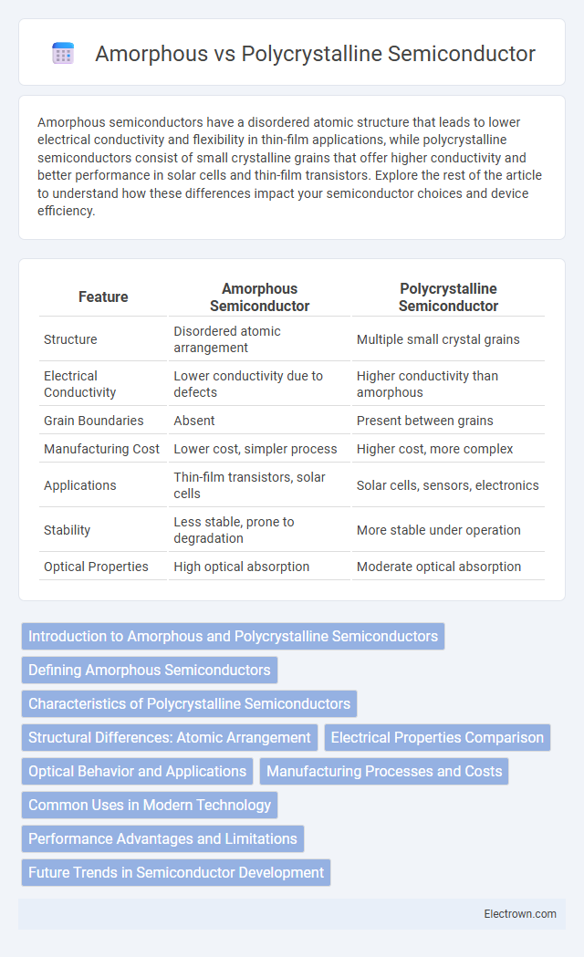
Table of Comparison
| Feature | Amorphous Semiconductor | Polycrystalline Semiconductor |
|---|---|---|
| Structure | Disordered atomic arrangement | Multiple small crystal grains |
| Electrical Conductivity | Lower conductivity due to defects | Higher conductivity than amorphous |
| Grain Boundaries | Absent | Present between grains |
| Manufacturing Cost | Lower cost, simpler process | Higher cost, more complex |
| Applications | Thin-film transistors, solar cells | Solar cells, sensors, electronics |
| Stability | Less stable, prone to degradation | More stable under operation |
| Optical Properties | High optical absorption | Moderate optical absorption |
Introduction to Amorphous and Polycrystalline Semiconductors
Amorphous semiconductors lack a long-range crystalline order, resulting in localized electronic states that influence their electrical and optical properties. Polycrystalline semiconductors consist of multiple small crystals or grains, separated by grain boundaries, which affect carrier mobility and recombination rates. Both materials are extensively used in thin-film technologies, such as solar cells and thin-film transistors, due to their unique structural and electronic characteristics.
Defining Amorphous Semiconductors
Amorphous semiconductors lack a long-range atomic order, distinguishing them from polycrystalline semiconductors with their ordered grain structures. These materials exhibit disordered atomic arrangements, leading to unique electronic properties such as localized states and variable band gaps. Common applications include thin-film transistors and solar cells, where flexible and cost-effective semiconductor layers are essential.
Characteristics of Polycrystalline Semiconductors
Polycrystalline semiconductors consist of multiple small crystalline grains separated by grain boundaries that influence electrical properties such as carrier mobility and recombination rates. These materials typically exhibit higher conductivity than amorphous semiconductors due to better structural order but lower than single-crystal counterparts. The grain boundaries act as defect sites, impacting charge carrier transport and overall device performance in applications like thin-film solar cells and TFT displays.
Structural Differences: Atomic Arrangement
Amorphous semiconductors exhibit a disordered atomic arrangement lacking long-range periodicity, resulting in random bonding and irregular lattice structures. Polycrystalline semiconductors consist of numerous small crystalline grains with well-ordered atomic arrangements within each grain, separated by grain boundaries. These structural differences impact electronic properties, with amorphous materials displaying localized states and polycrystalline materials having improved charge transport due to grain crystallinity.
Electrical Properties Comparison
Amorphous semiconductors exhibit lower electrical conductivity due to the presence of numerous localized states and defects that hinder charge carrier mobility compared to polycrystalline semiconductors, which have grain boundaries but generally allow better carrier transport. Polycrystalline materials display higher charge carrier mobility and improved electrical performance, making them suitable for devices requiring efficient current flow. Understanding these electrical property differences helps optimize your semiconductor selection for specific electronic and photovoltaic applications.
Optical Behavior and Applications
Amorphous semiconductors exhibit broad optical absorption due to their disordered atomic structure, making them ideal for thin-film solar cells and flexible electronic displays. Polycrystalline semiconductors offer higher optical transparency and improved charge transport, which enhances performance in photovoltaic devices and light-emitting diodes. Your choice between these materials depends on the specific optical requirements and application durability needed.
Manufacturing Processes and Costs
Amorphous semiconductors are produced through low-temperature deposition techniques such as chemical vapor deposition (CVD) or sputtering, which offer lower manufacturing costs due to simpler equipment and reduced energy consumption. Polycrystalline semiconductors require higher temperatures and more complex processes like crystallization annealing, increasing production time and expenses. Understanding these manufacturing differences helps optimize your choice for cost-effective semiconductor applications.
Common Uses in Modern Technology
Amorphous semiconductors are widely used in thin-film solar cells and flexible electronics due to their cost-effective production and adaptability to large-area substrates. Polycrystalline semiconductors, with higher electron mobility and efficiency, dominate in photovoltaic panels, power devices, and microelectronics where performance and reliability are critical. Your choice between these materials depends on the balance between manufacturing costs and device efficiency requirements.
Performance Advantages and Limitations
Amorphous semiconductors offer cost-effective fabrication and flexibility for thin-film applications but suffer from lower electron mobility and stability compared to crystalline counterparts. Polycrystalline semiconductors provide higher charge carrier mobility and better electrical performance, enhancing device efficiency in solar cells and thin-film transistors. However, grain boundaries in polycrystalline materials can introduce recombination sites, limiting overall performance and reliability.
Future Trends in Semiconductor Development
Future trends in semiconductor development emphasize the shift towards polycrystalline materials for enhanced electrical performance and durability compared to amorphous counterparts. Advances in manufacturing techniques are improving grain boundary control in polycrystalline semiconductors, boosting efficiency in solar cells and flexible electronics. Your applications will benefit from these innovations as devices become more reliable and energy-efficient in emerging technologies.
amorphous vs polycrystalline semiconductor Infographic