Grounded vias provide a direct electrical connection between different layers of a PCB and the ground plane, enhancing signal integrity and reducing electromagnetic interference. Understanding the distinctions between grounded and blind vias can help you optimize your PCB design; read on to explore their specific applications and benefits.
Table of Comparison
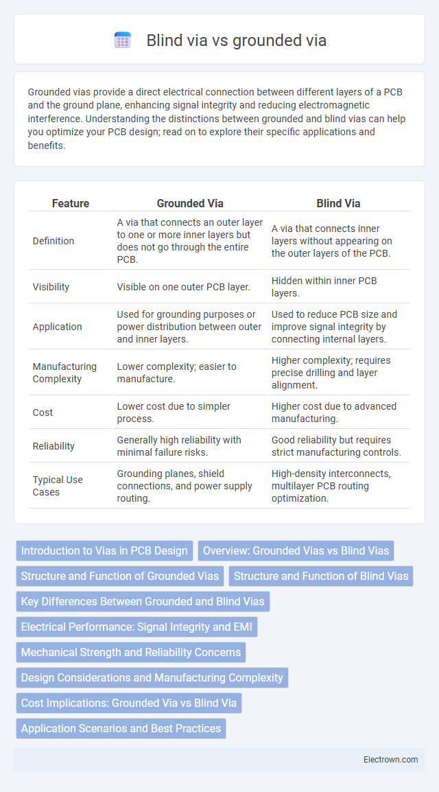
| Feature | Grounded Via | Blind Via |
|---|---|---|
| Definition | A via that connects an outer layer to one or more inner layers but does not go through the entire PCB. | A via that connects inner layers without appearing on the outer layers of the PCB. |
| Visibility | Visible on one outer PCB layer. | Hidden within inner PCB layers. |
| Application | Used for grounding purposes or power distribution between outer and inner layers. | Used to reduce PCB size and improve signal integrity by connecting internal layers. |
| Manufacturing Complexity | Lower complexity; easier to manufacture. | Higher complexity; requires precise drilling and layer alignment. |
| Cost | Lower cost due to simpler process. | Higher cost due to advanced manufacturing. |
| Reliability | Generally high reliability with minimal failure risks. | Good reliability but requires strict manufacturing controls. |
| Typical Use Cases | Grounding planes, shield connections, and power supply routing. | High-density interconnects, multilayer PCB routing optimization. |
Introduction to Vias in PCB Design
Vias in PCB design serve as electrical connections between different layers, enabling complex circuit routing. Grounded vias connect signals directly to the ground plane, enhancing signal integrity and reducing electromagnetic interference, while blind vias connect outer layers to internal layers without passing through the entire board, optimizing space and increasing routing density. Proper selection between grounded vias and blind vias is crucial for achieving optimal electrical performance and compact PCB layouts.
Overview: Grounded Vias vs Blind Vias
Grounded vias connect internal layers of a printed circuit board (PCB) to the ground plane, providing effective electromagnetic interference (EMI) shielding and improved signal integrity. Blind vias only connect outer layers to one or more inner layers without passing through the entire PCB, optimizing board space and enabling higher component density. Grounded vias enhance noise reduction in high-speed designs, while blind vias support complex multilayer layouts with better routing flexibility.
Structure and Function of Grounded Vias
Grounded vias are metal-filled holes connecting PCB layers to ground planes, providing essential electrical stability and noise reduction by minimizing electromagnetic interference (EMI). These vias maintain consistent impedance and improve signal integrity by offering a low-inductance return path for high-frequency signals. Understanding the structure and function of grounded vias helps you optimize PCB design for enhanced performance and reduced signal distortion.
Structure and Function of Blind Vias
Blind vias are short, vertical interconnections that connect an outer layer of a printed circuit board (PCB) to one or more inner layers without passing through the entire board, optimizing space and signal integrity. Structurally, blind vias are formed using laser drilling or mechanical drilling, followed by plating to ensure a conductive path confined within specified layers, which reduces parasitic inductance and capacitance compared to through-hole vias. Their primary function is to enhance high-density PCB designs by enabling efficient routing in multilayer boards without compromising mechanical stability or electrical performance.
Key Differences Between Grounded and Blind Vias
Grounded vias are electrically connected to a reference plane, providing effective noise reduction and improved signal integrity in multilayer PCBs, while blind vias connect only outer layers to specific inner layers without passing through the entire board, saving space and allowing for more complex circuit designs. You benefit from grounded vias when minimizing electromagnetic interference and enhancing grounding, whereas blind vias optimize board real estate and support higher component density. Choosing between grounded and blind vias depends on your PCB's electrical performance requirements and layout constraints.
Electrical Performance: Signal Integrity and EMI
Grounded VIAs significantly enhance electrical performance by providing a low-inductance return path, thereby improving signal integrity and reducing electromagnetic interference (EMI). Blind VIAs, while beneficial for saving PCB space, often introduce higher parasitic inductance and capacitance, which can degrade signal quality and increase EMI susceptibility. Optimizing the use of grounded VIAs is critical in high-speed designs to maintain signal integrity and ensure compliance with EMI standards.
Mechanical Strength and Reliability Concerns
Grounded vias provide enhanced mechanical strength and reliability by creating a secure electrical connection through multiple layers of the PCB, reducing stress concentration and improving structural integrity. Blind vias, while useful for space-saving in high-density designs, can introduce reliability concerns due to their limited depth and potential for weaker copper plating, increasing susceptibility to mechanical fatigue and failure. Your design choice should prioritize grounded vias when mechanical durability and long-term reliability are crucial for device performance.
Design Considerations and Manufacturing Complexity
Grounded vias provide enhanced electrical performance by connecting via barrels to a reference plane, reducing noise and signal interference, which demands precise alignment and additional etching steps during manufacturing. Blind vias, extending only partway into the substrate, optimize board space and improve high-density designs but increase complexity due to layer-specific drilling and plating processes. Your choice between grounded and blind vias should balance design requirements with the manufacturing capabilities to ensure cost-effectiveness and performance.
Cost Implications: Grounded Via vs Blind Via
Grounded vias generally incur higher manufacturing costs compared to blind vias due to the additional processes involved in plating and connecting to internal ground planes, enhancing electromagnetic interference control. Blind vias reduce material usage and layer-to-layer interconnections, lowering overall production expenses but may require more precise fabrication techniques. Your choice between grounded and blind vias should balance cost considerations against performance requirements in complex PCB designs.
Application Scenarios and Best Practices
Grounded vias are ideal for high-frequency applications and multi-layer PCBs where signal integrity and controlled impedance are critical, minimizing crosstalk and electromagnetic interference. Blind vias are best suited for space-constrained designs where connections are required between outer layers and one or more inner layers without penetrating the entire board, optimizing board real estate and improving reliability. For your PCB design, choose grounded vias in RF or high-speed circuits to enhance performance and blind vias in compact, multi-layer layouts to save space and maintain structural integrity.
grounded via vs blind via Infographic