FDSOI technology offers superior control over short-channel effects and reduced power consumption compared to Bulk CMOS, making it ideal for energy-efficient and high-performance applications. Discover how your choice between FDSOI and Bulk CMOS can impact device performance and design considerations in the full article.
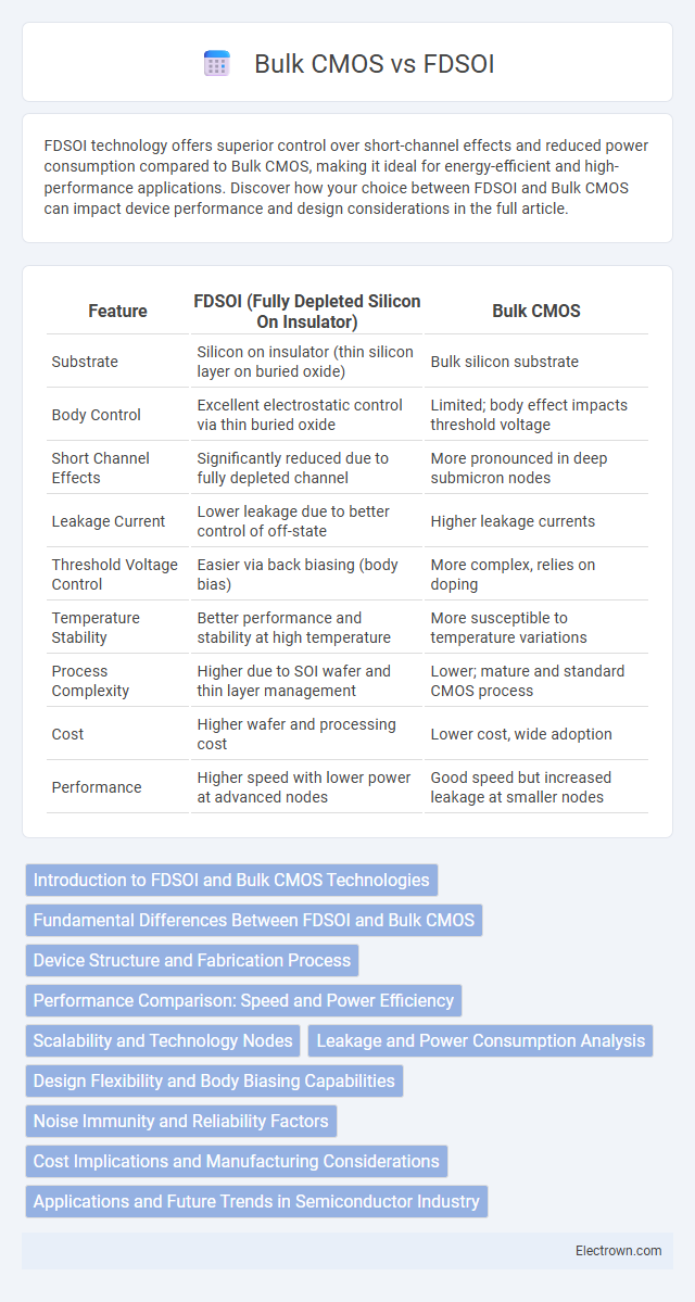
Table of Comparison
| Feature | FDSOI (Fully Depleted Silicon On Insulator) | Bulk CMOS |
|---|---|---|
| Substrate | Silicon on insulator (thin silicon layer on buried oxide) | Bulk silicon substrate |
| Body Control | Excellent electrostatic control via thin buried oxide | Limited; body effect impacts threshold voltage |
| Short Channel Effects | Significantly reduced due to fully depleted channel | More pronounced in deep submicron nodes |
| Leakage Current | Lower leakage due to better control of off-state | Higher leakage currents |
| Threshold Voltage Control | Easier via back biasing (body bias) | More complex, relies on doping |
| Temperature Stability | Better performance and stability at high temperature | More susceptible to temperature variations |
| Process Complexity | Higher due to SOI wafer and thin layer management | Lower; mature and standard CMOS process |
| Cost | Higher wafer and processing cost | Lower cost, wide adoption |
| Performance | Higher speed with lower power at advanced nodes | Good speed but increased leakage at smaller nodes |
Introduction to FDSOI and Bulk CMOS Technologies
FDSOI (Fully Depleted Silicon On Insulator) technology offers a thin silicon layer on an insulating substrate, enabling better electrostatic control and reduced leakage currents compared to Bulk CMOS, which uses a traditional silicon wafer with a thicker active layer. Bulk CMOS technology is widely used due to its maturity and cost-effectiveness, but FDSOI provides enhanced performance for low-power and high-speed applications by minimizing short-channel effects and improving scalability. Your choice between FDSOI and Bulk CMOS depends on specific needs for power efficiency, device density, and overall system performance.
Fundamental Differences Between FDSOI and Bulk CMOS
FDSOI (Fully Depleted Silicon On Insulator) technology features a thin silicon layer over a buried oxide, enabling improved electrostatic control and reduced short-channel effects compared to Bulk CMOS, which uses a thicker silicon substrate. FDSOI devices benefit from reduced leakage currents and lower power consumption due to their fully depleted channel, whereas Bulk CMOS relies on doped silicon channels with higher variability and increased leakage. The fundamental distinction lies in FDSOI's insulation layer that enhances device scalability and variability control, contrasting with Bulk CMOS's reliance on bulk silicon properties.
Device Structure and Fabrication Process
FD-SOI (Fully Depleted Silicon On Insulator) uses a thin silicon layer separated from the bulk substrate by a buried oxide layer, enabling better electrostatic control and reduced leakage currents compared to Bulk CMOS, which relies on a doped silicon substrate without an insulating layer. The FD-SOI fabrication process involves additional steps such as bonding and thinning the silicon layer, and integrating the buried oxide, while Bulk CMOS fabrication follows standard processes on bulk silicon wafers. FD-SOI's structure significantly improves device performance and scalability by minimizing short-channel effects and variability inherent in Bulk CMOS designs.
Performance Comparison: Speed and Power Efficiency
FD-SOI technology delivers superior speed and power efficiency compared to Bulk CMOS by utilizing a thin buried oxide layer that reduces parasitic capacitance and short-channel effects. This leads to enhanced transistor switching speeds while maintaining lower leakage currents, making FD-SOI optimal for low-power, high-performance applications. Bulk CMOS, although cost-effective, often suffers from higher power consumption and slower switching speeds due to increased leakage and reduced electrostatic control at advanced nodes.
Scalability and Technology Nodes
FDSOI technology enables enhanced scalability at advanced technology nodes down to 7nm and below, offering superior electrostatic control and reduced short-channel effects compared to Bulk CMOS. The ultra-thin buried oxide layer in FDSOI reduces variability and improves threshold voltage tuning, supporting better performance and power efficiency at smaller geometries. Bulk CMOS, while widely adopted, faces increased leakage and short-channel challenges as it scales beyond 14nm, limiting its effectiveness for future technology nodes.
Leakage and Power Consumption Analysis
FDSOI technology significantly reduces leakage current compared to Bulk CMOS due to its ultra-thin buried oxide layer that provides better electrostatic control of the channel, minimizing subthreshold leakage and gate-induced drain leakage. This control translates into lower static power consumption, making FDSOI highly advantageous for low-power applications and improving the overall energy efficiency of your designs. Leakage reduction in FDSOI also enables aggressive scaling and voltage scaling without compromising performance, further optimizing power consumption across various operating conditions.
Design Flexibility and Body Biasing Capabilities
FDSOI technology offers superior design flexibility through ultra-thin buried oxide layers enabling efficient dynamic body biasing for power and performance optimization. Bulk CMOS devices rely on substrate body biasing, but face limitations in controlling short-channel effects and leakage current compared to FDSOI. The inherent electrostatic control in FDSOI allows for wider voltage scaling and adaptive biasing techniques, enhancing device tunability across process corners and operating conditions.
Noise Immunity and Reliability Factors
FDSOI technology offers superior noise immunity compared to Bulk CMOS due to its ultra-thin buried oxide layer, which effectively isolates the transistor channel, reducing parasitic capacitance and minimizing voltage fluctuations. Reliability factors favor FDSOI because it exhibits lower variability and better control over short-channel effects, resulting in improved performance stability under temperature and voltage stress. Your design benefits from enhanced signal integrity and longer device lifespan when choosing FDSOI for noise-sensitive and reliability-critical applications.
Cost Implications and Manufacturing Considerations
FDSOI technology offers lower leakage currents and better electrostatic control than Bulk CMOS, which can reduce power consumption but typically incurs higher wafer costs due to specialized substrates. Bulk CMOS benefits from mature, high-volume manufacturing processes allowing for lower fabrication expenses and widespread adoption in diverse applications. Your choice between FDSOI and Bulk CMOS should weigh the trade-off between improved performance with FDSOI and the cost-effectiveness and scalability of Bulk CMOS manufacturing.
Applications and Future Trends in Semiconductor Industry
FDSOI technology offers superior electrostatic control and lower leakage currents, making it ideal for ultra-low power IoT devices, mobile processors, and automotive electronics where energy efficiency is critical. Bulk CMOS, with its mature manufacturing ecosystem and cost-effectiveness, remains the preferred choice for high-volume applications such as consumer electronics and general-purpose computing. Future trends indicate a growing adoption of FDSOI in mixed-signal and RF applications, leveraging its analog performance benefits, while advanced bulk CMOS nodes continue to scale with FinFET and Gate-All-Around technologies to meet the demands of high-performance computing and AI workloads.
FDSOI vs Bulk CMOS Infographic