Blind vias connect inner layers to outer layers without passing through the entire circuit board, saving space and improving signal integrity, while buried vias link only internal layers, hidden from the external surfaces, ideal for complex multi-layer PCBs. Understanding these distinctions helps you optimize your PCB design for performance and reliability; read on to explore their specific applications and benefits.
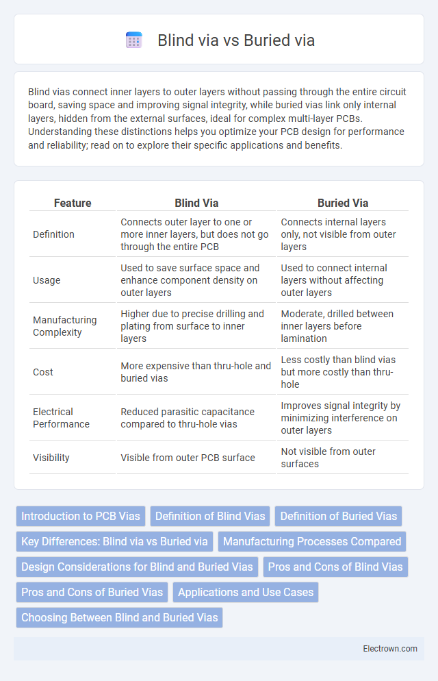
Table of Comparison
| Feature | Blind Via | Buried Via |
|---|---|---|
| Definition | Connects outer layer to one or more inner layers, but does not go through the entire PCB | Connects internal layers only, not visible from outer layers |
| Usage | Used to save surface space and enhance component density on outer layers | Used to connect internal layers without affecting outer layers |
| Manufacturing Complexity | Higher due to precise drilling and plating from surface to inner layers | Moderate, drilled between inner layers before lamination |
| Cost | More expensive than thru-hole and buried vias | Less costly than blind vias but more costly than thru-hole |
| Electrical Performance | Reduced parasitic capacitance compared to thru-hole vias | Improves signal integrity by minimizing interference on outer layers |
| Visibility | Visible from outer PCB surface | Not visible from outer surfaces |
Introduction to PCB Vias
Blind vias in printed circuit boards (PCBs) connect outer layers to one or more inner layers without passing through the entire board, optimizing space and improving signal integrity in high-density designs. Buried vias are entirely encapsulated within the inner layers, invisible from the outer layers, enhancing multi-layer PCB complexity and enabling compact routing. Both via types address specific electrical and design challenges, playing critical roles in advanced PCB manufacturing processes.
Definition of Blind Vias
Blind vias are electrical connections in printed circuit boards (PCBs) that link outer layers to one or more inner layers without passing through the entire board thickness, enhancing signal integrity and saving space. Buried vias, by contrast, connect only inner layers and remain completely enclosed within the PCB, invisible from both external surfaces. The use of blind vias optimizes high-density interconnections in multilayer PCBs, especially in complex electronic devices such as smartphones and aerospace equipment.
Definition of Buried Vias
Buried vias are electrical connections that link internal layers of a printed circuit board (PCB) without extending to the outer layers, remaining hidden within the board's core. Unlike blind vias, which connect an outer layer to one or more inner layers but do not pass through the entire board, buried vias contribute to higher circuit density and reduce surface space usage by being embedded entirely inside the PCB. The implementation of buried vias is critical in multilayer PCBs to enhance electrical performance while minimizing electromagnetic interference and signal loss.
Key Differences: Blind via vs Buried via
Blind vias connect an outer PCB layer to an inner layer without passing through the entire board, optimizing space and signal integrity in high-density designs. Buried vias, however, only connect internal layers and are completely enclosed within the PCB, invisible from both outer surfaces, enhancing layer isolation and reducing crosstalk. The key difference lies in their visibility and connectivity: blind vias link outer layers to inner layers, while buried vias connect only internal layers, influencing PCB design complexity and manufacturing costs.
Manufacturing Processes Compared
Blind vias connect an outer layer to one or more inner layers without going through the entire PCB, requiring precise laser drilling or mechanical drilling processes that minimize board thickness and improve signal integrity. Buried vias connect only inner layers and are completely encapsulated within the PCB, necessitating sequential lamination and advanced drilling techniques to maintain layer alignment and reliability. Choosing between blind and buried vias influences manufacturing complexity, cost, and electrical performance, making it essential to align your design requirements with the appropriate via type.
Design Considerations for Blind and Buried Vias
Design considerations for blind and buried vias center on optimizing PCB layer interconnectivity while minimizing signal loss and manufacturing complexity. Blind vias connect outer layers to one or more inner layers without passing through the entire board, requiring precise drilling depth control and plating quality to ensure reliability. Buried vias are fully enclosed within inner layers, demanding meticulous layout planning to maintain electrical performance and avoid interference with adjacent circuitry or mechanical stability.
Pros and Cons of Blind Vias
Blind vias enhance PCB density by connecting outer layers to inner layers without penetrating the entire board, allowing for more compact and complex circuit designs. The main advantages include increased routing space, reduced signal path lengths, and improved electrical performance, while drawbacks involve higher manufacturing costs, increased complexity in fabrication, and potential reliability issues due to the difficulty in inspecting these vias. Choosing blind vias requires balancing improved design flexibility against the added expenses and fabrication challenges.
Pros and Cons of Buried Vias
Buried vias enhance PCB design by saving surface space and enabling higher wiring density, critical for multi-layer boards in advanced electronics. However, buried vias increase manufacturing complexity and cost due to additional drilling and inspection steps, potentially impacting yield rates. Their limited accessibility complicates testing and repair, making careful design and process control essential to balance performance benefits against production challenges.
Applications and Use Cases
Blind via technology is widely used in high-density printed circuit boards (PCBs) to connect an outer layer to one or more inner layers without traversing the entire board, optimizing real estate in compact electronic devices like smartphones and laptops. Buried vias connect only internal layers, making them essential in multilayer PCBs for complex circuits in applications such as aerospace, medical devices, and high-speed computing where signal integrity and board space are critical. Both technologies enhance electrical performance and reliability by reducing parasitic capacitance and inductance, supporting advanced circuit designs in aerospace, telecommunications, automotive electronics, and consumer gadgets.
Choosing Between Blind and Buried Vias
Choosing between blind and buried vias depends on PCB design complexity and layer count. Blind vias connect outer layers to internal layers without passing through the entire board, ideal for high-density designs and maintaining signal integrity. Buried vias connect only internal layers, optimizing space in multilayer boards but requiring more precise manufacturing, influencing cost and reliability.
Blind via vs Buried via Infographic