Shrink and node migration are key techniques for optimizing data storage and improving cluster performance in distributed systems. Explore the rest of the article to understand how these methods impact your infrastructure efficiency and scalability.
Table of Comparison
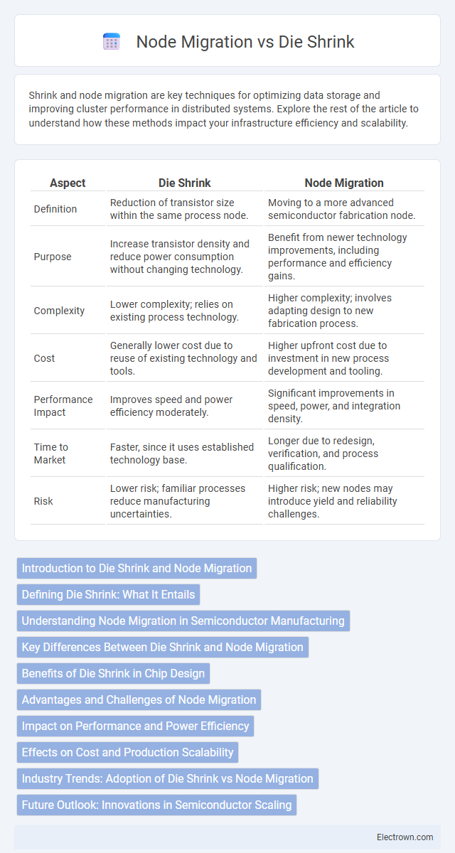
| Aspect | Die Shrink | Node Migration |
|---|---|---|
| Definition | Reduction of transistor size within the same process node. | Moving to a more advanced semiconductor fabrication node. |
| Purpose | Increase transistor density and reduce power consumption without changing technology. | Benefit from newer technology improvements, including performance and efficiency gains. |
| Complexity | Lower complexity; relies on existing process technology. | Higher complexity; involves adapting design to new fabrication process. |
| Cost | Generally lower cost due to reuse of existing technology and tools. | Higher upfront cost due to investment in new process development and tooling. |
| Performance Impact | Improves speed and power efficiency moderately. | Significant improvements in speed, power, and integration density. |
| Time to Market | Faster, since it uses established technology base. | Longer due to redesign, verification, and process qualification. |
| Risk | Lower risk; familiar processes reduce manufacturing uncertainties. | Higher risk; new nodes may introduce yield and reliability challenges. |
Introduction to Die Shrink and Node Migration
Die Shrink refers to the process of reducing the physical dimensions of semiconductor components to fit more transistors onto a single chip, enhancing performance and energy efficiency. Node Migration involves transitioning from one semiconductor manufacturing process node to a smaller, more advanced node, enabling higher transistor density and improved chip capabilities. Both techniques are critical in advancing integrated circuit technology, with Die Shrink focusing on miniaturization within the same node and Node Migration representing a shift to a new fabrication process.
Defining Die Shrink: What It Entails
Die shrink refers to the process of reducing the size of a semiconductor chip's components to fit more transistors into a smaller physical area, enhancing performance and energy efficiency. This technique involves using advanced lithography technologies to shrink feature sizes on the silicon wafer, enabling higher transistor density without drastically redesigning the underlying architecture. Your devices benefit from improved speed and reduced power consumption due to the miniaturization that die shrink achieves.
Understanding Node Migration in Semiconductor Manufacturing
Node migration in semiconductor manufacturing refers to the strategic process of transitioning chip production from one technology node to another, typically to improve performance, reduce power consumption, and lower manufacturing costs. Unlike die shrink, which involves miniaturizing the transistor size within the same process technology, node migration encompasses adopting new lithography techniques, materials, and design architectures to advance overall semiconductor capabilities. This migration often requires significant retooling and design recalibration to optimize yields and meet the demands of evolving electronic applications.
Key Differences Between Die Shrink and Node Migration
Die Shrink involves reducing the physical dimensions of semiconductor components within the same manufacturing process node, enhancing transistor density and power efficiency. Node Migration transitions the fabrication process to a smaller technology node, introducing significant changes in materials, design rules, and transistor architectures. Understanding these key differences helps optimize your chip design strategy by balancing improved performance with cost and complexity considerations.
Benefits of Die Shrink in Chip Design
Die shrink in chip design significantly enhances performance by reducing transistor size, enabling higher speed and lower power consumption. It increases chip density, allowing more functionality and complexity in the same silicon area, reducing costs per chip. Improved thermal efficiency and yield rates are other critical benefits, driving advancements in semiconductor technology.
Advantages and Challenges of Node Migration
Node migration offers significant advantages such as enhanced load balancing, improved fault tolerance, and minimized downtime during system upgrades or maintenance. It enables seamless transfer of processes across nodes, optimizing resource utilization and maintaining high availability in distributed computing environments. Challenges include ensuring data consistency, handling network latency, and managing complex synchronization mechanisms to prevent process interruption or failure during migration.
Impact on Performance and Power Efficiency
Die shrink reduces transistor size, enhancing performance by enabling higher clock speeds and increased transistor density, which simultaneously lowers power consumption due to decreased capacitance and voltage requirements. Node migration, involving shifting designs to a different process node, can improve or deteriorate power efficiency and performance based on design compatibility and process characteristics. Optimizing for die shrink maximizes both performance gains and power efficiency, while node migration demands careful evaluation to avoid potential trade-offs.
Effects on Cost and Production Scalability
Die shrink significantly reduces manufacturing costs by increasing wafer yield and decreasing material usage, enabling higher production scalability through smaller, more efficient chip designs. Node migration often incurs higher initial expenses due to new equipment and design complexities but offers long-term cost benefits with improved performance and power efficiency. Both strategies impact production scalability differently: die shrink boosts volume and yield on existing nodes, while node migration facilitates access to advanced technology nodes for cutting-edge applications.
Industry Trends: Adoption of Die Shrink vs Node Migration
The semiconductor industry increasingly favors die shrink techniques to enhance chip performance and reduce manufacturing costs by leveraging smaller process nodes without the need for complete node migration. Die shrink adoption accelerates as it offers quicker time-to-market advantages while preserving design architecture, making it a preferred strategy over costly and complex node migration. Your choice between die shrink and node migration will depend on balancing performance gains against development resources in line with current industry trends.
Future Outlook: Innovations in Semiconductor Scaling
Die Shrink and Node Migration remain pivotal strategies in semiconductor scaling, driving advancements in transistor density and power efficiency. Emerging innovations such as extreme ultraviolet (EUV) lithography and gate-all-around (GAA) transistor architectures enhance the feasibility of smaller nodes beyond 3nm. Future outlooks predict a blend of incremental die shrinks combined with node migration to 2nm and below, enabling continued performance gains while addressing challenges in heat dissipation and manufacturing complexity.
Die Shrink vs Node Migration Infographic