Ohmic contacts provide low-resistance, linear current-voltage characteristics essential for efficient charge injection in nanoscale junctions, while Schottky contacts form rectifying barriers that control carrier flow through energy band tuning. Understanding the distinct electrical behaviors and fabrication techniques of these contacts can enhance your ability to optimize nanoscale device performance--explore the detailed comparison in the following sections.
Table of Comparison
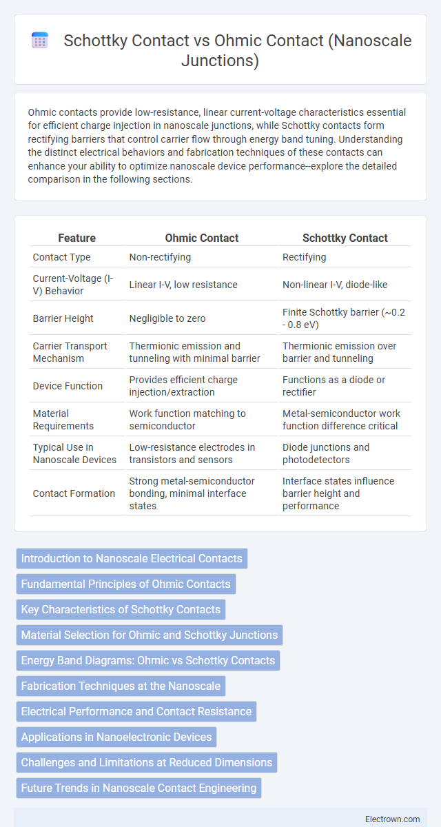
| Feature | Ohmic Contact | Schottky Contact |
|---|---|---|
| Contact Type | Non-rectifying | Rectifying |
| Current-Voltage (I-V) Behavior | Linear I-V, low resistance | Non-linear I-V, diode-like |
| Barrier Height | Negligible to zero | Finite Schottky barrier (~0.2 - 0.8 eV) |
| Carrier Transport Mechanism | Thermionic emission and tunneling with minimal barrier | Thermionic emission over barrier and tunneling |
| Device Function | Provides efficient charge injection/extraction | Functions as a diode or rectifier |
| Material Requirements | Work function matching to semiconductor | Metal-semiconductor work function difference critical |
| Typical Use in Nanoscale Devices | Low-resistance electrodes in transistors and sensors | Diode junctions and photodetectors |
| Contact Formation | Strong metal-semiconductor bonding, minimal interface states | Interface states influence barrier height and performance |
Introduction to Nanoscale Electrical Contacts
Nanoscale electrical contacts, pivotal in modern electronics, differ significantly between ohmic and Schottky contacts in terms of charge carrier transport and barrier formation. Ohmic contacts provide low-resistance, linear current-voltage behavior, facilitating efficient charge injection without energy barriers, essential for minimizing contact resistance in nanoscale devices. In contrast, Schottky contacts form a rectifying junction with a built-in potential barrier at the metal-semiconductor interface, significantly influencing device characteristics such as current rectification and sensitivity in nanoscale field-effect transistors and sensors.
Fundamental Principles of Ohmic Contacts
Ohmic contacts in nanoscale junctions provide a low-resistance, linear current-voltage relationship by ensuring efficient charge carrier injection between metal and semiconductor. Their fundamental principle is based on minimizing energy barriers at the interface, often achieved through heavy doping or selecting metals with work functions closely matched to the semiconductor's conduction or valence band. Understanding these principles helps you optimize device performance by reducing contact resistance and enhancing signal integrity in nanoelectronic applications.
Key Characteristics of Schottky Contacts
Schottky contacts in nanoscale junctions are characterized by a rectifying behavior with a built-in potential barrier formed at the metal-semiconductor interface, facilitating unidirectional current flow. These contacts exhibit lower forward voltage drops compared to ohmic contacts, but higher contact resistance and nonlinear current-voltage characteristics due to the Schottky barrier height. The barrier height and interface states critically influence the charge transport mechanism, impacting device performance in nanoelectronic applications.
Material Selection for Ohmic and Schottky Junctions
Material selection for ohmic contacts in nanoscale junctions typically involves metals with work functions closely matched to the semiconductor's conduction or valence band to minimize barrier height, such as Ti/Au for n-type GaAs. Schottky contacts rely on metals with comparatively higher or lower work functions to create a rectifying barrier, for example, Pt or Ni on n-type silicon to form a Schottky barrier. Optimizing your contact material enhances device performance by ensuring efficient charge carrier injection or controlled barrier formation essential for nanoscale applications.
Energy Band Diagrams: Ohmic vs Schottky Contacts
Energy band diagrams of ohmic contacts exhibit a negligible energy barrier at the metal-semiconductor interface, allowing for seamless charge carrier flow and minimal contact resistance. Schottky contacts, however, display a significant energy barrier (Schottky barrier) that impedes carrier injection, resulting in rectifying behavior. Your understanding of nanoscale junction performance hinges on recognizing how these distinct band alignments influence current conduction and device efficiency.
Fabrication Techniques at the Nanoscale
Fabrication techniques for ohmic contacts at the nanoscale often involve precise deposition methods such as electron beam evaporation, sputtering, or atomic layer deposition to achieve low-resistance, non-rectifying interfaces with materials like metals (e.g., Ti/Au, Ni/Au) on semiconductor nanostructures. Schottky contacts require controlled metal-semiconductor interface engineering, using techniques like focused ion beam milling or molecular beam epitaxy to form rectifying junctions with defined barrier heights, often involving metals such as Pt or Pd on nanoscale silicon or III-V semiconductor devices. Nanoscale patterning and surface treatment processes, including plasma etching or rapid thermal annealing, are critical to modulate contact properties and minimize interface states for both ohmic and Schottky contacts.
Electrical Performance and Contact Resistance
Ohmic contacts in nanoscale junctions offer low contact resistance and linear current-voltage characteristics, enabling efficient charge carrier injection with minimal energy loss. Schottky contacts exhibit rectifying behavior with higher contact resistance, arising from the Schottky barrier formed at the metal-semiconductor interface, which impedes charge flow in one direction. Your device performance depends heavily on selecting the appropriate contact type to optimize electrical conductivity and minimize power dissipation in nanoscale electronic components.
Applications in Nanoelectronic Devices
Ohmic contacts in nanoscale junctions provide low-resistance, linear current-voltage characteristics essential for efficient charge injection in nanoelectronic devices such as field-effect transistors and sensors. Schottky contacts form rectifying junctions with diode-like behavior, enabling applications in high-speed switching, photodetectors, and nanogenerators by exploiting their barrier-dependent charge transport properties. Optimizing the contact type directly influences device performance, power consumption, and switching speed in advanced nanoscale electronic architectures.
Challenges and Limitations at Reduced Dimensions
Nanoscale Ohmic contacts face challenges like increased contact resistance due to quantum confinement and surface roughness, which degrade electron transport efficiency. Schottky contacts exhibit variability in barrier height at reduced dimensions, causing inconsistent current flow and enhanced leakage currents from tunneling effects. Both contact types struggle with fabrication precision and maintaining interface stability as device scaling approaches atomic limits.
Future Trends in Nanoscale Contact Engineering
Future trends in nanoscale contact engineering emphasize the development of ultra-low resistance Ohmic contacts using novel 2D materials like graphene and transition metal dichalcogenides to enhance device performance. Schottky contacts are being optimized through precise work function engineering and atomic-scale interface control to tailor barrier heights in next-generation nanoelectronic devices. Your ability to integrate these advanced contact architectures will drive improvements in energy efficiency, speed, and scalability in semiconductor and optoelectronic applications.
Ohmic contact vs Schottky contact (nanoscale junctions) Infographic