Sub-10nm FinFET technology offers improved transistor density and enhanced power efficiency compared to earlier nodes, while 7nm FinFET further pushes performance boundaries with superior speed and reduced energy consumption for advanced applications. Explore the detailed comparison to understand which technology best suits your design and performance needs.
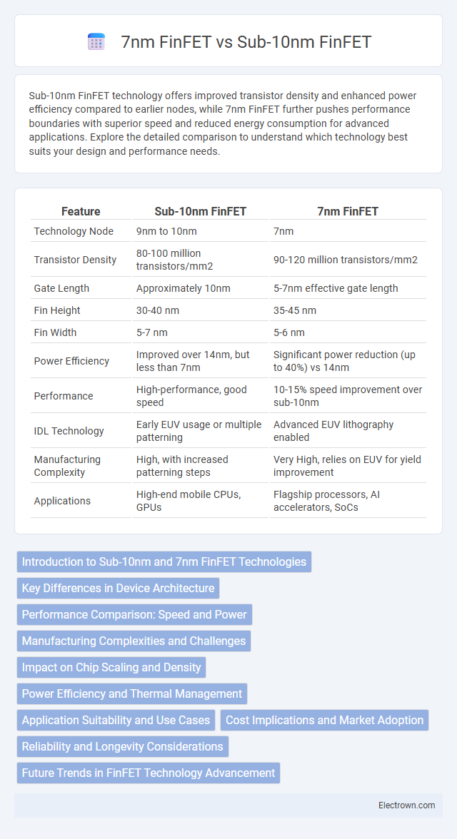
Table of Comparison
| Feature | Sub-10nm FinFET | 7nm FinFET |
|---|---|---|
| Technology Node | 9nm to 10nm | 7nm |
| Transistor Density | 80-100 million transistors/mm2 | 90-120 million transistors/mm2 |
| Gate Length | Approximately 10nm | 5-7nm effective gate length |
| Fin Height | 30-40 nm | 35-45 nm |
| Fin Width | 5-7 nm | 5-6 nm |
| Power Efficiency | Improved over 14nm, but less than 7nm | Significant power reduction (up to 40%) vs 14nm |
| Performance | High-performance, good speed | 10-15% speed improvement over sub-10nm |
| IDL Technology | Early EUV usage or multiple patterning | Advanced EUV lithography enabled |
| Manufacturing Complexity | High, with increased patterning steps | Very High, relies on EUV for yield improvement |
| Applications | High-end mobile CPUs, GPUs | Flagship processors, AI accelerators, SoCs |
Introduction to Sub-10nm and 7nm FinFET Technologies
Sub-10nm and 7nm FinFET technologies represent advanced transistor nodes in semiconductor manufacturing, characterized by their enhanced electrostatic control and reduced short-channel effects. The 7nm FinFET process leverages extreme ultraviolet (EUV) lithography for finer patterning, enabling higher transistor density and improved power efficiency compared to earlier nodes. You benefit from the increased performance and energy savings these technologies offer, essential for high-performance computing and mobile applications.
Key Differences in Device Architecture
Sub-10nm FinFET devices integrate advanced multi-gate structures with reduced fin pitch and gate length compared to 7nm FinFETs, enabling enhanced electrostatic control and reduced short-channel effects. The sub-10nm technology often employs new materials like high-mobility channels and ultra-thin high-k dielectrics to maintain performance scaling and power efficiency. Enhanced patterning techniques such as extreme ultraviolet (EUV) lithography are critical in achieving the tighter geometries and improved device density characteristic of sub-10nm FinFET architectures.
Performance Comparison: Speed and Power
Sub-10nm FinFET technology offers higher transistor density and improved short-channel control compared to 7nm FinFET, resulting in enhanced speed due to reduced gate length and lower parasitic capacitance. Power consumption in sub-10nm nodes is significantly optimized through advanced electrostatic control and lower leakage currents, enabling better power efficiency at comparable or higher operating frequencies than 7nm FinFET devices. These improvements contribute to faster switching speeds and reduced dynamic power, making sub-10nm FinFETs more suitable for high-performance and low-power applications.
Manufacturing Complexities and Challenges
Sub-10nm FinFET technology faces increased manufacturing complexities due to extreme ultraviolet (EUV) lithography requirements, tighter design rules, and diminished process margins compared to 7nm FinFET. The reduction in gate length and fin spacing demands advanced patterning techniques and more precise etching processes, raising defect density risks and yield challenges. Managing variability in channel doping and fin height uniformity intensifies as transistor geometries shrink below 10nm, complicating process control and increasing production costs relative to established 7nm nodes.
Impact on Chip Scaling and Density
Sub-10nm FinFET technology enhances chip scaling by enabling smaller transistor footprints compared to 7nm FinFET, resulting in higher transistor density and improved performance per watt. The reduced gate length and fin dimensions allow more logic elements to fit within the same silicon area, directly boosting chip complexity and functional integration. This increased density also facilitates advanced packaging solutions, supporting more efficient multi-core and heterogeneous system-on-chip architectures.
Power Efficiency and Thermal Management
Sub-10nm FinFET technology offers enhanced power efficiency compared to 7nm FinFET due to reduced leakage currents and improved transistor switching characteristics, enabling lower voltage operation. Thermal management benefits from the smaller node's optimized gate control and reduced short-channel effects, resulting in lower heat generation and improved device reliability. Your choice of Sub-10nm FinFET can lead to significant gains in energy savings and cooler device performance, crucial for high-performance computing applications.
Application Suitability and Use Cases
Sub-10nm FinFET technology offers enhanced power efficiency and higher transistor density, making it ideal for ultra-mobile devices and edge computing applications where energy consumption is critical. 7nm FinFET remains widely used in high-performance computing, servers, and gaming GPUs due to its mature manufacturing process and balanced power-performance characteristics. Your choice between these nodes should consider the specific application's performance demands and energy efficiency requirements.
Cost Implications and Market Adoption
Sub-10nm FinFET technology demands significantly higher manufacturing costs due to increased complexity and advanced lithography processes, impacting your budget for semiconductor production. In contrast, 7nm FinFET offers a more balanced cost-to-performance ratio, leading to broader market adoption across consumer electronics and high-performance computing sectors. Market trends indicate stronger adoption of 7nm nodes as they provide cost-effective scaling with improved power efficiency, making them favorable for mainstream applications.
Reliability and Longevity Considerations
Sub-10nm FinFET technology offers advancements in transistor scaling but introduces new challenges in reliability due to increased variability and susceptibility to short-channel effects compared to 7nm FinFET. The 7nm FinFET process generally provides more mature defect control and enhanced thermal management, contributing to longer device longevity and stable performance under extended operational stress. For Your applications requiring dependable performance, 7nm FinFETs often deliver superior reliability and lifespan, whereas sub-10nm designs may necessitate additional mitigation techniques to ensure durability.
Future Trends in FinFET Technology Advancement
Sub-10nm FinFET technology emphasizes extreme scaling with enhanced gate control and reduced short-channel effects, pushing transistor density beyond 100 million per mm2. The 7nm FinFET process, primarily driven by EUV lithography, offers improved power efficiency and performance scaling, enabling advanced SoCs for AI and 5G applications. Future trends include transitioning to nanosheet and gate-all-around (GAA) architectures beyond sub-5nm nodes, integrating advanced materials like high-mobility channels, and employing multi-patterning techniques for further dimensional control.
Sub-10nm FinFET vs 7nm FinFET Infographic