Enhancement load refers to the additional genetic burden caused by mutations that intensify the effects of existing deleterious alleles, while depletion load arises from the loss of beneficial alleles reducing population fitness. Understanding the balance between these two loads is crucial for interpreting evolutionary dynamics and managing genetic health; explore the article to learn how these concepts impact your study or conservation efforts.
Table of Comparison
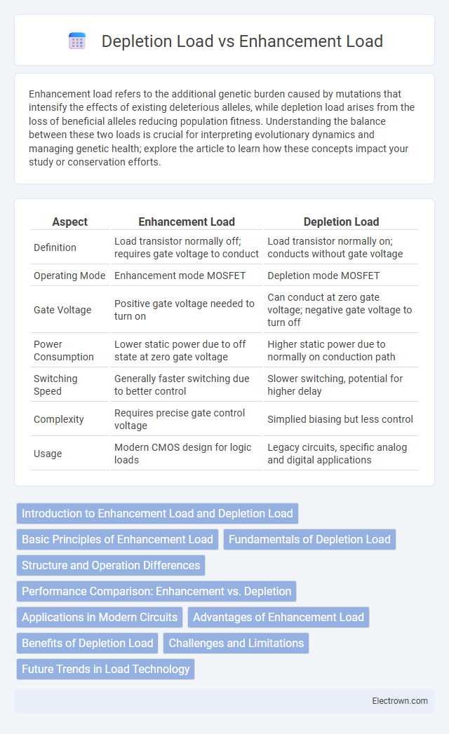
| Aspect | Enhancement Load | Depletion Load |
|---|---|---|
| Definition | Load transistor normally off; requires gate voltage to conduct | Load transistor normally on; conducts without gate voltage |
| Operating Mode | Enhancement mode MOSFET | Depletion mode MOSFET |
| Gate Voltage | Positive gate voltage needed to turn on | Can conduct at zero gate voltage; negative gate voltage to turn off |
| Power Consumption | Lower static power due to off state at zero gate voltage | Higher static power due to normally on conduction path |
| Switching Speed | Generally faster switching due to better control | Slower switching, potential for higher delay |
| Complexity | Requires precise gate control voltage | Simplied biasing but less control |
| Usage | Modern CMOS design for logic loads | Legacy circuits, specific analog and digital applications |
Introduction to Enhancement Load and Depletion Load
Enhancement load and depletion load refer to two fundamental types of MOSFET operation modes characterized by the gate voltage relative to the threshold voltage. Enhancement load devices require a positive gate-to-source voltage to create a conductive channel, functioning as normally off switches with no current flow at zero gate bias. Depletion load devices possess a conductive channel at zero gate bias and require a negative gate-to-source voltage to deplete the channel and turn off the current flow.
Basic Principles of Enhancement Load
Enhancement load refers to the increase in electrical current required to switch a MOSFET transistor from the off state to the on state by applying a positive gate voltage, fundamental to the operation of enhancement-mode devices. This load is characterized by the threshold voltage that must be surpassed to form a conductive channel between the source and drain, allowing current flow. Your circuit design must consider this basic principle to ensure efficient switching performance and power consumption in enhancement-mode MOSFET applications.
Fundamentals of Depletion Load
Depletion load refers to the reduction of soil nutrients and minerals due to continuous cropping or improper land management, leading to decreased soil fertility and productivity. This process involves the removal of essential macro and micronutrients faster than their natural replenishment through organic matter decomposition or fertilization. Understanding depletion load is crucial for implementing sustainable agricultural practices that balance nutrient inputs and outputs to maintain soil health over time.
Structure and Operation Differences
Enhancement load MOSFETs utilize an insulated gate structure that controls channel formation by applying a positive gate voltage, creating a conductive path between source and drain, while depletion load MOSFETs have a built-in channel at zero gate voltage and operate by depleting carriers with a negative gate voltage. The enhancement load device remains normally off without gate bias, enabling lower static power consumption, whereas the depletion load device is normally on due to its intrinsic channel, leading to continuous current flow even when the gate is unbiased. Structurally, enhancement load transistors rely on inducing inversion layers for conduction, while depletion load transistors depend on doping profiles to maintain a channel without gate drive.
Performance Comparison: Enhancement vs. Depletion
Enhancement load MOSFETs typically offer higher switching speeds and lower on-resistance compared to depletion load MOSFETs, leading to improved overall circuit performance in digital applications. Depletion load transistors operate with normally-on characteristics, which may increase static power consumption but provide a simpler design for certain analog circuits. Performance comparison shows enhancement loads excel in speed and power efficiency, while depletion loads benefit from reduced complexity and stable operation under specific conditions.
Applications in Modern Circuits
Enhancement load transistors are widely used in CMOS logic circuits due to their high noise margins and low static power consumption, making them ideal for digital applications requiring energy efficiency and reliability. Depletion load devices, often found in older NMOS logic families, provide a constant current load that simplifies circuit design but typically result in higher power dissipation and smaller voltage swings. Modern integrated circuits favor enhancement load configurations for their superior scalability, reduced leakage currents, and compatibility with low-voltage operation in advanced semiconductor technologies.
Advantages of Enhancement Load
Enhancement load transistors offer advantages such as lower power consumption and higher switching speeds compared to depletion load transistors. Their ability to remain normally off reduces static power dissipation, making them ideal for low-power integrated circuits. Enhanced control over threshold voltage enables better noise margins and improved overall circuit reliability.
Benefits of Depletion Load
Depletion load circuits offer significant benefits including reduced static power consumption and improved noise margins, making them ideal for low-power applications. They enable simpler circuit design by eliminating the need for an external resistor, which enhances integration density and reduces overall chip area. Their high impedance load characteristic provides better voltage swing and faster switching speeds compared to enhancement load configurations.
Challenges and Limitations
Enhancement load techniques face challenges such as increased power consumption and complexity in transistor design, limiting their scalability in low-power applications. Depletion load designs encounter limitations due to reduced drive current and slower switching speeds, impacting overall circuit performance and efficiency. Both methods must address trade-offs between speed, power, and device reliability to optimize integrated circuit functionality.
Future Trends in Load Technology
Enhancement load MOSFETs dominate future trends due to their higher efficiency, faster switching speeds, and lower leakage currents compared to depletion load devices. Innovations in semiconductor materials and nanofabrication techniques are driving the development of enhancement load transistors tailored for high-performance and low-power applications. Your choice of load technology will increasingly favor enhancement load MOSFETs to meet the demands of next-generation electronics.
Enhancement load vs depletion load Infographic