Deep trench isolation offers superior electrical isolation and reduced capacitance in high-density integrated circuits compared to shallow trench isolation, which is simpler but less effective in minimizing leakage currents. Explore the article to understand how these trench isolation techniques impact your semiconductor device performance and design choices.
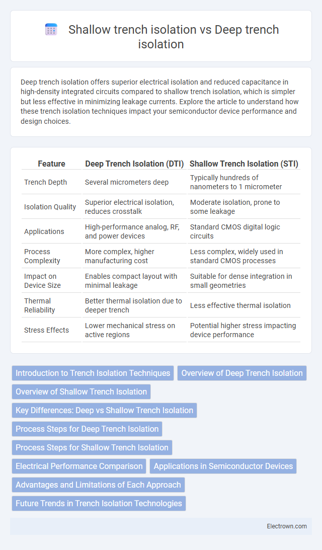
Table of Comparison
| Feature | Deep Trench Isolation (DTI) | Shallow Trench Isolation (STI) |
|---|---|---|
| Trench Depth | Several micrometers deep | Typically hundreds of nanometers to 1 micrometer |
| Isolation Quality | Superior electrical isolation, reduces crosstalk | Moderate isolation, prone to some leakage |
| Applications | High-performance analog, RF, and power devices | Standard CMOS digital logic circuits |
| Process Complexity | More complex, higher manufacturing cost | Less complex, widely used in standard CMOS processes |
| Impact on Device Size | Enables compact layout with minimal leakage | Suitable for dense integration in small geometries |
| Thermal Reliability | Better thermal isolation due to deeper trench | Less effective thermal isolation |
| Stress Effects | Lower mechanical stress on active regions | Potential higher stress impacting device performance |
Introduction to Trench Isolation Techniques
Trench isolation techniques, including deep trench isolation (DTI) and shallow trench isolation (STI), are essential for electrically isolating semiconductor devices to prevent leakage currents and crosstalk in integrated circuits. Shallow trench isolation involves etching narrow and shallow trenches filled with dielectric materials, commonly silicon dioxide, to separate devices at the surface level, suitable for CMOS technology nodes above 65 nm. Deep trench isolation creates deeper and narrower trenches, enhancing isolation in DRAM capacitors and advanced memory devices by reducing parasitic capacitance and substrate coupling more effectively than STI.
Overview of Deep Trench Isolation
Deep Trench Isolation (DTI) involves etching deep, narrow trenches into the semiconductor substrate to electrically isolate devices and reduce parasitic capacitance, significantly improving performance in high-density integrated circuits. You achieve superior electrical isolation and enhanced device scaling compared to Shallow Trench Isolation (STI), which uses shallower trenches filled with insulating material. DTI is especially beneficial in analog, RF, and high-voltage applications where minimizing leakage and crosstalk is critical.
Overview of Shallow Trench Isolation
Shallow Trench Isolation (STI) is a semiconductor device fabrication technique used to electrically isolate individual transistors on a silicon wafer by etching shallow trenches filled with an insulating material, typically silicon dioxide. STI offers advantages in minimizing leakage currents and improving device uniformity by effectively preventing electrical crosstalk between components. Your integrated circuits benefit from STI's precision and scalability, especially in advanced CMOS technologies where device density and performance are critical.
Key Differences: Deep vs Shallow Trench Isolation
Deep trench isolation (DTI) provides superior electrical isolation by creating trenches several micrometers deep, effectively reducing parasitic capacitance and leakage currents in high-performance semiconductor devices. Shallow trench isolation (STI), with trenches typically less than one micrometer deep, is commonly used for planar devices to prevent current leakage between adjacent transistors while maintaining a compact footprint. Your choice between DTI and STI depends on device requirements, with DTI favored for advanced, high-density circuits needing robust isolation and STI suitable for cost-effective, standard applications.
Process Steps for Deep Trench Isolation
Deep trench isolation (DTI) involves etching deep, narrow trenches into the silicon substrate using reactive ion etching (RIE), followed by filling these trenches with dielectric materials such as silicon dioxide or silicon nitride to electrically isolate regions. The process requires precise photolithography to define trench patterns, thermal oxidation to grow a thin oxide liner for interface passivation, and chemical mechanical polishing (CMP) to planarize the surface after trench fill. DTI offers superior isolation for advanced semiconductor devices by minimizing parasitic capacitance and leakage compared to shallow trench isolation (STI), making it critical for high-voltage and high-performance applications.
Process Steps for Shallow Trench Isolation
Shallow trench isolation (STI) involves etching a narrow trench into the silicon substrate, followed by growing a thin oxide liner and depositing silicon dioxide to fill the trench. Chemical mechanical polishing (CMP) planarizes the wafer surface, ensuring uniformity and preventing electrical leakage. This process enhances device performance by providing effective isolation between transistors while minimizing silicon area loss compared to deep trench isolation.
Electrical Performance Comparison
Deep trench isolation (DTI) offers superior electrical performance by significantly reducing parasitic capacitance and leakage currents compared to shallow trench isolation (STI). The increased depth of DTI improves device isolation, minimizes crosstalk, and enhances signal integrity, which is critical for advanced semiconductor technologies. STI, while effective for moderate isolation, exhibits higher parasitics and less efficient suppression of substrate interactions, making DTI preferable for high-performance and low-power applications.
Applications in Semiconductor Devices
Deep trench isolation (DTI) is extensively used in high-voltage and power semiconductor devices to provide superior electrical isolation and minimize substrate coupling, enhancing device reliability and performance. Shallow trench isolation (STI) is commonly applied in low-voltage CMOS integrated circuits, offering efficient isolation with minimized parasitic capacitance for high-density microelectronic chip fabrication. Your choice between DTI and STI depends on the specific device requirements, such as voltage levels, integration density, and performance targets.
Advantages and Limitations of Each Approach
Deep trench isolation offers superior electrical isolation and reduced parasitic capacitance, enhancing device performance and scalability in advanced semiconductor nodes. However, it involves complex fabrication processes and higher costs, with potential issues like stress-induced defects affecting device reliability. Shallow trench isolation provides simpler manufacturing, lower cost, and adequate isolation for less dense circuits, but it suffers from higher leakage currents and limited effectiveness in high-voltage or high-frequency applications.
Future Trends in Trench Isolation Technologies
Deep trench isolation (DTI) is gaining traction for its superior electrical isolation and reduced parasitic capacitance, making it ideal for advanced semiconductor nodes below 5 nm. Shallow trench isolation (STI) still plays a critical role in mature technology nodes due to its lower production complexity and cost-effectiveness. Emerging trends indicate a hybrid approach leveraging the benefits of both DTI and STI will dominate, driven by demands for higher device density, improved performance, and reduced power consumption in future integrated circuits.
Deep trench vs Shallow trench isolation Infographic