Pull-up and pull-down networks form the foundation of CMOS logic circuits by controlling the output voltage through PMOS and NMOS transistors, respectively. Understanding how these networks work together to switch and drive the output is essential for optimizing your circuit's performance and power consumption--explore the rest of this article to dive deeper into their functions and design considerations.
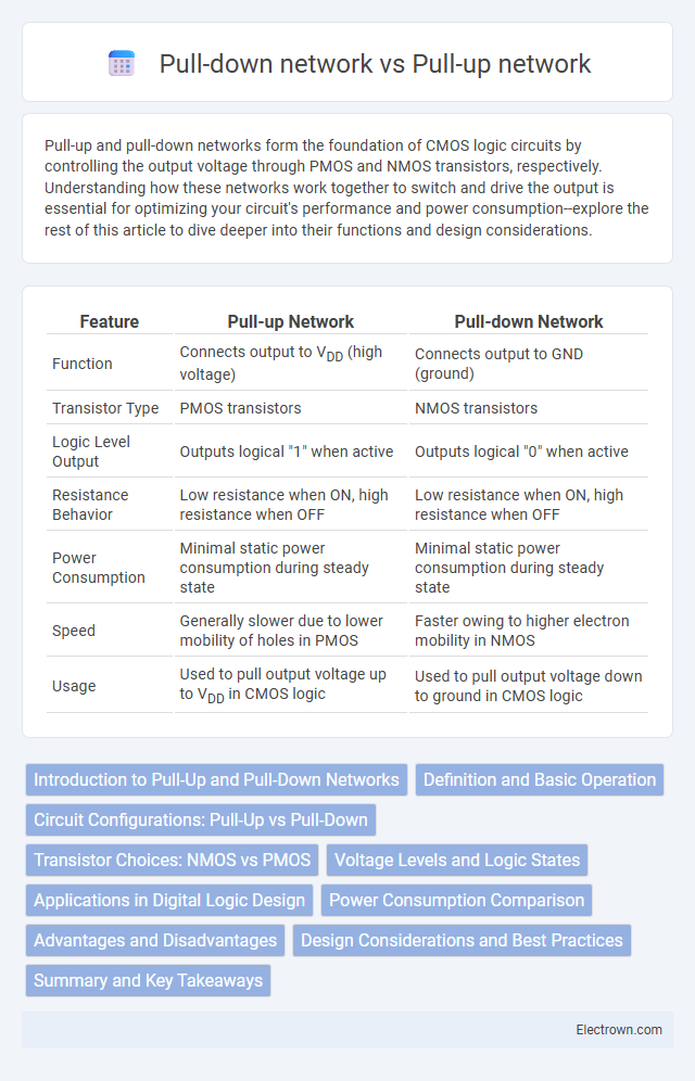
Table of Comparison
| Feature | Pull-up Network | Pull-down Network |
|---|---|---|
| Function | Connects output to VDD (high voltage) | Connects output to GND (ground) |
| Transistor Type | PMOS transistors | NMOS transistors |
| Logic Level Output | Outputs logical "1" when active | Outputs logical "0" when active |
| Resistance Behavior | Low resistance when ON, high resistance when OFF | Low resistance when ON, high resistance when OFF |
| Power Consumption | Minimal static power consumption during steady state | Minimal static power consumption during steady state |
| Speed | Generally slower due to lower mobility of holes in PMOS | Faster owing to higher electron mobility in NMOS |
| Usage | Used to pull output voltage up to VDD in CMOS logic | Used to pull output voltage down to ground in CMOS logic |
Introduction to Pull-Up and Pull-Down Networks
Pull-up and pull-down networks are fundamental components in CMOS logic design, responsible for driving the output to a high or low voltage level. The pull-up network consists of p-type MOSFETs that connect the output to the positive supply voltage, ensuring a logic high output, while the pull-down network uses n-type MOSFETs to connect the output to ground, resulting in a logic low output. Understanding the complementary operation of these networks is crucial for designing efficient digital circuits with minimal power consumption and fast switching speeds.
Definition and Basic Operation
Pull-up networks consist of PMOS transistors connected to the positive supply voltage, ensuring the output node is driven high when activated. Pull-down networks use NMOS transistors connected to ground, pulling the output node low when engaged. Both networks form complementary structures in CMOS logic gates to control output voltage levels efficiently.
Circuit Configurations: Pull-Up vs Pull-Down
Pull-up networks use PMOS transistors connected to the power supply to ensure a high output voltage when activated, while pull-down networks utilize NMOS transistors connected to ground to pull the output low. The configuration of pull-up circuits typically involves sourcing current, whereas pull-down circuits sink current, enabling complementary behavior in CMOS technology. Your understanding of these circuit configurations is essential for designing efficient logic gates with balanced switching characteristics.
Transistor Choices: NMOS vs PMOS
Pull-up networks primarily use PMOS transistors due to their ability to conduct strongly when pulling the output voltage to VDD, benefiting from low resistance in the on-state. In contrast, pull-down networks employ NMOS transistors because they offer better electron mobility, enabling efficient conduction to ground with faster switching performance. The complementary use of PMOS in pull-up and NMOS in pull-down configurations optimizes overall CMOS inverter speed, power consumption, and noise margins.
Voltage Levels and Logic States
Pull-up networks connect the output to a high voltage level (V_DD) ensuring a logic high (1) when the transistor is off, while pull-down networks connect the output to ground (0 V) to produce a logic low (0) when active. The voltage level at the output node depends on whether the pull-up NMOS transistors or pull-down PMOS transistors are conducting, establishing clear logic states without floating nodes. Understanding these voltage behaviors helps you design reliable CMOS circuits with well-defined logic thresholds and minimal noise susceptibility.
Applications in Digital Logic Design
Pull-up and pull-down networks form the fundamental building blocks of CMOS digital logic circuits, where pull-up networks use p-type MOSFETs to connect the output to V_DD, and pull-down networks use n-type MOSFETs to connect the output to ground. Their complementary action ensures low power consumption and robust noise margins, critical for applications like inverters, NAND gates, and NOR gates in digital logic design. Your circuit's performance and power efficiency depend on the precise arrangement and switching of these networks, making them essential for creating reliable combinational and sequential logic devices.
Power Consumption Comparison
Pull-up networks, typically constructed with PMOS transistors, exhibit lower static power consumption due to minimal leakage currents when in the off state, while pull-down networks using NMOS transistors generally consume more power during switching because of higher electron mobility and faster operation. However, pull-down networks can lead to increased dynamic power consumption due to larger capacitive loads and higher switching frequencies. Optimizing the balance between PMOS and NMOS transistor sizing and threshold voltages is critical to minimizing overall power consumption in CMOS logic gate design.
Advantages and Disadvantages
Pull-up networks, typically using PMOS transistors, provide strong logic high levels and low static power consumption but tend to exhibit slower switching speeds compared to pull-down networks made of NMOS transistors. Pull-down networks excel in faster switching and stronger logic low output, though they consume higher static power and require more complex design considerations to avoid ground bounce and noise. Combining both networks in CMOS technology optimizes circuit performance by leveraging the strengths of pull-up and pull-down configurations while mitigating their individual disadvantages.
Design Considerations and Best Practices
Pull-up and pull-down networks are critical in CMOS logic design, influencing switching speed, power consumption, and noise margins. Optimizing transistor sizing ensures balanced rise and fall times, enhancing signal integrity and minimizing static power dissipation in Your circuits. Proper layout and avoiding excessive stacking in these networks prevent increased delay and leakage, resulting in efficient and robust digital designs.
Summary and Key Takeaways
Pull-up and pull-down networks form the complementary parts of CMOS logic gates, where the pull-up network uses PMOS transistors to connect the output to VDD, and the pull-down network uses NMOS transistors to connect the output to ground. The efficiency of CMOS circuits relies on the complementary action of both networks, ensuring low power consumption and fast switching by avoiding direct path conduction between power and ground. Understanding the design and operation of these networks is crucial for optimizing digital circuit performance, power efficiency, and noise margins in integrated circuit design.
Pull-up vs Pull-down network Infographic