Conventional MOSFETs face challenges in scaling due to short-channel effects and increased leakage current, whereas FinFETs offer improved electrostatic control and reduced power consumption by using a 3D fin-shaped channel structure. Discover how these differences impact your device performance and future semiconductor technology in the rest of the article.
Table of Comparison
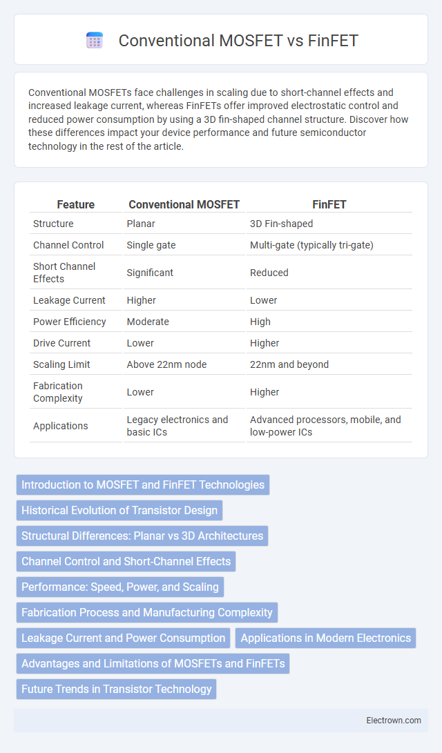
| Feature | Conventional MOSFET | FinFET |
|---|---|---|
| Structure | Planar | 3D Fin-shaped |
| Channel Control | Single gate | Multi-gate (typically tri-gate) |
| Short Channel Effects | Significant | Reduced |
| Leakage Current | Higher | Lower |
| Power Efficiency | Moderate | High |
| Drive Current | Lower | Higher |
| Scaling Limit | Above 22nm node | 22nm and beyond |
| Fabrication Complexity | Lower | Higher |
| Applications | Legacy electronics and basic ICs | Advanced processors, mobile, and low-power ICs |
Introduction to MOSFET and FinFET Technologies
MOSFET technology relies on a planar structure to control current flow through a single gate over a flat channel, making it fundamental in traditional semiconductor devices. FinFET technology improves upon this by employing a three-dimensional fin-like channel wrapped by multiple gates, enhancing control over leakage currents and enabling better performance at smaller nanometer scales. Your choice between conventional MOSFETs and FinFETs depends on the requirements for power efficiency, switching speed, and scalability in modern integrated circuits.
Historical Evolution of Transistor Design
The historical evolution of transistor design showcases the transition from Conventional MOSFETs, pioneered in the 1960s with planar structures, to FinFET technology introduced in the mid-2000s to address short-channel effects and leakage currents in nanoscale devices. Conventional MOSFETs evolved through scaling innovations like the introduction of high-k dielectrics and strained silicon to improve performance, yet faced limitations in power efficiency and control at smaller nodes. FinFETs revolutionized transistor architecture by enabling three-dimensional channels, offering enhanced electrostatic control, reduced leakage, and superior performance for modern semiconductor technologies crucial to advancing your device capabilities.
Structural Differences: Planar vs 3D Architectures
Conventional MOSFETs use planar architecture with a flat, two-dimensional channel, which limits gate control and increases leakage current as device size shrinks. FinFETs incorporate a 3D structure with a vertical fin-shaped channel wrapped by the gate, enhancing electrostatic control and reducing short-channel effects. This structural difference allows FinFETs to achieve higher drive current, improved scalability, and lower power consumption compared to planar MOSFETs.
Channel Control and Short-Channel Effects
FinFET technology offers superior channel control compared to conventional MOSFETs by utilizing a 3D fin-shaped channel that surrounds the gate on multiple sides, significantly reducing leakage currents and enhancing electrostatic control. Conventional MOSFETs suffer more from short-channel effects, such as threshold voltage roll-off and drain-induced barrier lowering, due to their planar structure and weaker gate control. Your device's performance and power efficiency improve substantially with FinFETs, especially as transistor dimensions continue to scale below 20 nm.
Performance: Speed, Power, and Scaling
FinFETs outperform conventional MOSFETs by offering significantly higher switching speeds due to improved channel control and reduced short-channel effects, enabling faster transistor operation. Power efficiency in FinFETs is enhanced through lower leakage currents and reduced power consumption at smaller nodes, supporting energy-efficient designs in modern integrated circuits. FinFET technology allows better scaling beyond 14nm, overcoming the physical limitations faced by planar MOSFETs, thus facilitating continued transistor density increases and performance improvements in advanced semiconductor processes.
Fabrication Process and Manufacturing Complexity
Conventional MOSFETs utilize a planar structure with a relatively straightforward fabrication process, relying on photolithography and ion implantation techniques that have been well-established for decades. FinFETs feature a three-dimensional, fin-like channel that requires advanced multi-patterning and precise etching methods, significantly increasing manufacturing complexity and cost. Your choice between these technologies impacts fabrication scalability, yield, and integration with cutting-edge nodes below 10 nm.
Leakage Current and Power Consumption
Conventional MOSFETs exhibit higher leakage current due to their planar structure, which leads to increased power consumption, especially in low-voltage applications. FinFET technology reduces leakage current significantly by using a 3D fin-shaped channel that provides better gate control, improving energy efficiency. Your devices can achieve lower power consumption and enhanced performance with FinFETs, making them ideal for advanced semiconductor applications.
Applications in Modern Electronics
Conventional MOSFETs remain widely used in power electronics and analog circuits due to their simplicity and cost-effectiveness, making them ideal for applications requiring low-frequency operation and high voltage tolerance. FinFET technology, with its superior electrostatic control and reduced short-channel effects, dominates high-performance processors, mobile devices, and advanced integrated circuits where power efficiency and scaling are critical. Your choice between these transistor types depends on specific performance requirements, thermal constraints, and integration density in modern electronic designs.
Advantages and Limitations of MOSFETs and FinFETs
MOSFETs offer simplicity, low cost, and well-established manufacturing processes but face limitations like increased short-channel effects and leakage current at nanoscale dimensions. FinFETs provide superior control over channel electrostatics, reducing leakage and enhancing performance for advanced nodes below 22nm, yet they involve higher fabrication complexity and cost. The transition from conventional MOSFETs to FinFETs enables continued device scaling and improved power efficiency in modern integrated circuits.
Future Trends in Transistor Technology
Future trends in transistor technology emphasize the shift from Conventional MOSFETs to FinFETs due to FinFETs' superior electrostatic control and reduced short-channel effects, enabling further scaling below 10 nm nodes. You can expect continued innovation in 3D transistor architectures, such as Gate-All-Around (GAA) FETs, to enhance performance while minimizing power consumption in advanced semiconductor manufacturing. Industry leaders are focusing on integrating these technologies to meet demands for higher speed, lower power, and improved energy efficiency in next-generation processors and memory devices.
Conventional MOSFET vs FinFET Infographic