Fanout PCBs distribute signals evenly across multiple layers to improve signal integrity and reduce interference, making them ideal for complex, high-density designs. Breakout PCBs simplify routing by separating dense pin arrays into accessible traces, enhancing manufacturability and testing; explore the article to determine which approach best suits your project needs.
Table of Comparison
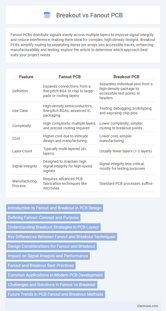
| Feature | Fanout PCB | Breakout PCB |
|---|---|---|
| Definition | Expands connections from a fine-pitch BGA or chip to larger pads or routing layers | Separates individual pins from a high-density package to accessible test points or headers |
| Use Case | High-density semiconductors, fine-pitch BGAs, advanced IC packaging | Testing, debugging, prototyping, and exposing chip pins |
| Complexity | High complexity; multiple layers and precise routing required | Lower complexity; simpler routing to breakout points |
| Cost | Higher cost due to intricate design and manufacturing | Lower cost, simpler manufacturing |
| Layer Count | Typically multi-layered (4+ layers) | Usually fewer layers (1-2 layers) |
| Signal Integrity | Designed to maintain high signal integrity for high-speed signals | Signal integrity less critical; mostly for testing purposes |
| Manufacturing Process | Requires advanced PCB fabrication techniques like microvias | Standard PCB processes suffice |
Introduction to Fanout and Breakout in PCB Design
Fanout in PCB design refers to the technique of routing traces from densely packed BGA (Ball Grid Array) pads to accessible vias or component pins to ensure signal integrity and manufacturability. Breakout is the process of dispersing signals from a single dense component, like a BGA or fine-pitch device, to surrounding space or layers for easier routing and testing. Both fanout and breakout strategies are essential for optimizing space, improving electrical performance, and enabling layer transitions in complex PCB layouts.
Defining Fanout: Concept and Purpose
Fanout in PCB design refers to the technique of routing traces from a fine-pitch BGA or similar component to larger pads or vias, enabling easier soldering and electrical connections. This method optimizes signal integrity and manufacturability by efficiently distributing pins across the PCB layers. Understanding fanout helps you ensure reliable performance and facilitates assembly in complex multi-layer boards.
Understanding Breakout Strategies in PCB Layout
Breakout strategies in PCB layout are crucial for managing component pin connections, where fanout involves routing traces from a dense array of pins to larger spacing for easier routing. Breakout PCBs facilitate signal breakout by converting fine-pitch or BGA pads into accessible pads or vias, improving manufacturability and signal integrity. Your choice between fanout and breakout depends on factors like component density, layer count, and desired electrical performance.
Key Differences Between Fanout and Breakout Techniques
Fanout PCB technology spreads the I/O pads of a chip over a larger area using redistribution layers, enhancing high-density interconnections and improving signal integrity for advanced semiconductor packages. Breakout PCB techniques route signals from densely packed pads to a wider pitch, simplifying connections to external components and reducing design complexity. Understanding these key differences allows you to optimize PCB layouts for performance, manufacturing ease, and application-specific requirements.
Design Considerations for Fanout and Breakout
Design considerations for fanout and breakout PCBs revolve around signal integrity, component density, and manufacturability. Fanout PCB design requires careful pad spacing and controlled impedance to manage high-density BGA components, while breakout PCB focuses on routing traces from board edges or connectors with ample clearance to ensure reliable signal paths. Your choice impacts layer count, trace length, and overall electrical performance, demanding precise planning during schematic and layout stages.
Impact on Signal Integrity and Performance
Fanout PCBs enhance signal integrity by reducing via stubs and impedance discontinuities, leading to improved high-frequency performance and minimized signal reflections. Breakout PCBs facilitate better trace routing from dense BGA pads, limiting crosstalk and maintaining signal timing critical for high-speed data transmission. Optimizing fanout and breakout design directly impacts electromagnetic compatibility and overall PCB reliability in advanced electronic systems.
Fanout and Breakout Best Practices
Fanout PCB design maximizes signal routing by spreading chip pads outward to larger routing channels, improving manufacturability and signal integrity. Breakout PCB designs focus on efficiently routing signals from dense pin arrays to wider pitch areas, minimizing crosstalk and impedance mismatches. Best practices for fanout and breakout include maintaining consistent trace impedance, using staggered vias to reduce stress, and optimizing pad size for reliable solder joints and signal performance.
Common Applications in Modern PCB Development
Fanout PCBs are primarily used in high-density applications such as smartphones and advanced wearable devices, where efficient signal routing and reduced package size are critical. Breakout PCBs are commonly found in testing environments and development boards, providing accessible connections for prototyping and debugging. Both technologies play essential roles in accelerating product development cycles within consumer electronics and IoT industries.
Challenges and Solutions in Fanout vs Breakout
Fanout and breakout PCB designs each present unique challenges; fanout requires managing high-density routing with minimal signal crosstalk, while breakout boards face constraints in limited space for component placement and trace routing. Solutions for fanout include advanced via-in-pad techniques and microvia technology to optimize signal integrity and reduce board size. For breakout PCBs, employing strategic component arrangement and multi-layer routing ensures efficient connectivity and mitigates electrical interference, enhancing Your PCB's performance.
Future Trends in PCB Fanout and Breakout Methods
Future trends in PCB fanout and breakout methods emphasize increased use of high-density interconnect (HDI) technology and advanced via structures like microvias and stacked vias to enhance signal integrity and miniaturization. Emerging materials with better thermal and electrical performance are driving improved reliability in fanout designs, while breakout methods are evolving to support higher layer counts and complex multilayer routing. Your PCB designs will benefit from these innovations by achieving greater functionality in smaller form factors, meeting the demands of next-generation electronics.
fanout vs breakout PCB Infographic