A wafer is a thin, circular slice of semiconductor material, typically silicon, used as the substrate for integrated circuits, while a die refers to the individual rectangular or square pieces cut from the wafer that become the actual chips in electronic devices. Understanding the differences between wafer and die is essential for optimizing your semiconductor manufacturing process--explore the rest of this article to learn more.
Table of Comparison
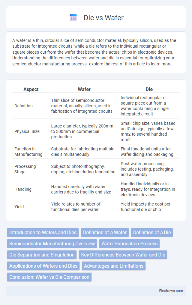
| Aspect | Wafer | Die |
|---|---|---|
| Definition | Thin slice of semiconductor material, usually silicon, used in fabrication of integrated circuits | Individual rectangular or square piece cut from a wafer containing a single integrated circuit |
| Physical Size | Large diameter, typically 200mm to 300mm in commercial production | Small chip size, varies based on IC design, typically a few mm2 to several hundred mm2 |
| Function in Manufacturing | Substrate for fabricating multiple dies simultaneously | Final functional units after wafer dicing and packaging |
| Processing Stage | Subject to photolithography, doping, etching during fabrication | Post wafer processing, includes testing, packaging, and assembly |
| Handling | Handled carefully with wafer carriers due to fragility and size | Handled individually or in trays, ready for integration in electronic devices |
| Yield | Yield relates to number of functional dies per wafer | Yield impacts the cost per functional die or chip |
Introduction to Wafers and Dies
Wafers are thin slices of semiconductor material, typically silicon, used as the foundational substrate in microelectronics fabrication. Dies are individual rectangular or square chips cut from a wafer, each containing an integrated circuit that performs specific electronic functions. The manufacturing process converts wafers into multiple dies through photolithography and etching steps essential for producing microchips.
Definition of a Wafer
A wafer is a thin, flat slice of semiconductor material, typically silicon, used as the substrate for microelectronic devices. It serves as the foundational platform from which multiple dies, or individual integrated circuits, are fabricated through photolithography and etching processes. Understanding the wafer's role is essential for managing your semiconductor manufacturing workflow and optimizing device yield.
Definition of a Die
A die refers to a small, individual block of semiconducting material, typically silicon, cut from a larger wafer to create a single integrated circuit. It contains the complete electronic circuitry required for a specific function, such as a microprocessor or memory chip. Your device's performance depends on the quality and precision of the dies produced during the semiconductor manufacturing process.
Semiconductor Manufacturing Overview
In semiconductor manufacturing, a wafer is a thin slice of semiconductor material, typically silicon, used as the substrate for fabricating integrated circuits. Multiple dies, or individual chips, are patterned onto each wafer through processes such as photolithography, etching, and doping. After processing, the wafer is diced into separate dies, which are then packaged and tested for use in electronic devices.
Wafer Fabrication Process
The wafer fabrication process involves creating semiconductor wafers from a single crystal silicon boule, which are then sliced into thin discs called wafers. Each wafer undergoes multiple photolithography, etching, doping, and deposition steps to build integrated circuits layer by layer before being diced into individual dies. Understanding this process helps you grasp why wafer quality directly impacts the yield and performance of the final semiconductor dies used in electronic devices.
Die Separation and Singulation
Die separation and singulation involve cutting individual dies from a semiconductor wafer, typically using techniques such as mechanical sawing, laser cutting, or plasma etching. Precision in singulation ensures minimal damage to dies while maximizing yield and maintaining electrical performance. Advanced methods like stealth dicing create defect-free edges, enhancing the reliability of integrated circuits in final applications.
Key Differences Between Wafer and Die
A wafer is a thin, circular slice of semiconductor material used as the substrate for fabricating integrated circuits, while a die is an individual rectangular or square chip cut from the wafer that contains a complete functional circuit. Wafers typically range from 100 mm to 300 mm in diameter and contain dozens to thousands of dies depending on their size. The key difference lies in scale and function: wafers serve as the manufacturing platform, whereas dies are the final individual units tested and packaged for electronic devices.
Applications of Wafers and Dies
Wafers serve as the foundational substrates in semiconductor manufacturing, enabling the production of integrated circuits for smartphones, computers, and automotive electronics. Dies, which are individual chips cut from wafers, are used directly in electronic devices such as microprocessors, memory chips, and sensors. The precise fabrication of wafers ensures high yield and performance in dies, critical for applications in consumer electronics, medical devices, and industrial automation.
Advantages and Limitations
Wafers enable mass production of semiconductor devices, offering cost efficiency and uniformity through simultaneous fabrication of multiple dies. Die provide flexibility for customized or prototype circuits but face higher per-unit costs and potential variability in performance. Optimizing Your manufacturing approach depends on balancing wafer-scale economies against die-level customization needs.
Conclusion: Wafer vs Die Comparison
Wafer and die serve distinct roles in semiconductor manufacturing, with wafers acting as the original silicon substrate and dies representing the individual integrated circuits cut from the wafer. Your choice between focusing on wafers or dies depends on whether you prioritize large-scale fabrication processes or detailed component-level analysis. Understanding the differences is crucial for optimizing production efficiency and ensuring high-quality semiconductor products.
wafer vs die Infographic