Gallium nitride (GaN) offers superior power efficiency and high thermal stability, making it ideal for high-frequency and high-power applications, while gallium arsenide (GaAs) excels in high-speed electronics and optoelectronics due to its superior electron mobility. Discover how choosing between GaN and GaAs can directly impact your device performance by exploring the rest of the article.
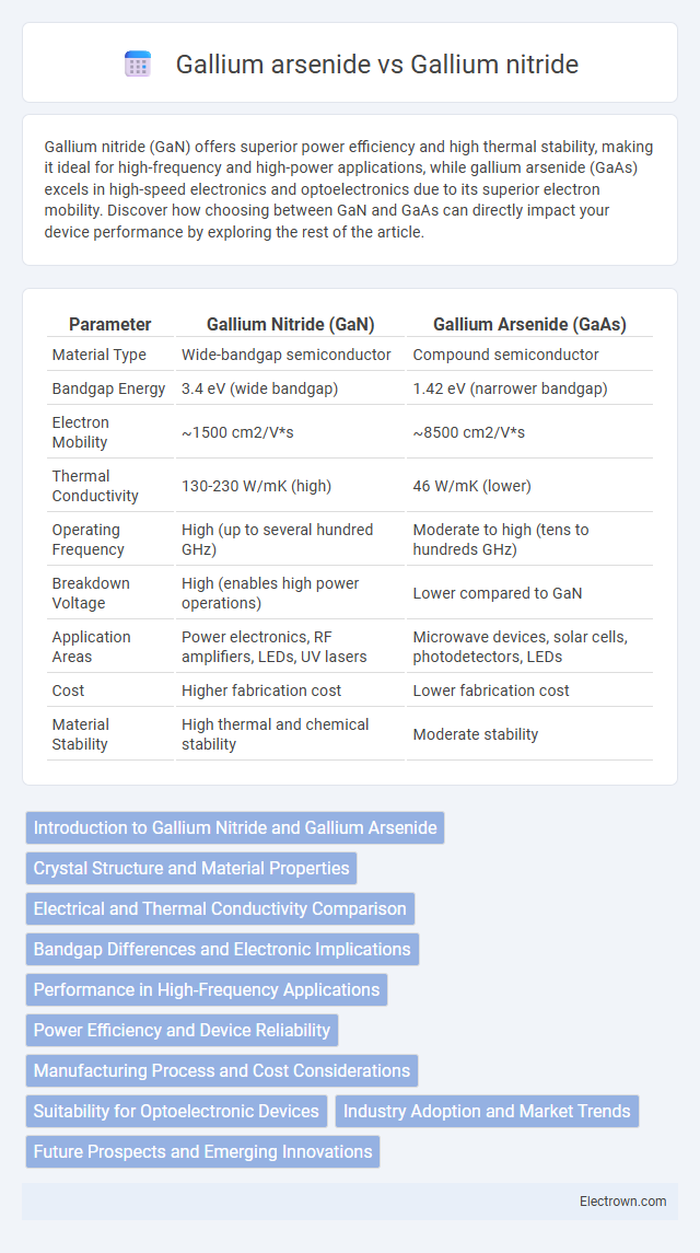
Table of Comparison
| Parameter | Gallium Nitride (GaN) | Gallium Arsenide (GaAs) |
|---|---|---|
| Material Type | Wide-bandgap semiconductor | Compound semiconductor |
| Bandgap Energy | 3.4 eV (wide bandgap) | 1.42 eV (narrower bandgap) |
| Electron Mobility | ~1500 cm2/V*s | ~8500 cm2/V*s |
| Thermal Conductivity | 130-230 W/mK (high) | 46 W/mK (lower) |
| Operating Frequency | High (up to several hundred GHz) | Moderate to high (tens to hundreds GHz) |
| Breakdown Voltage | High (enables high power operations) | Lower compared to GaN |
| Application Areas | Power electronics, RF amplifiers, LEDs, UV lasers | Microwave devices, solar cells, photodetectors, LEDs |
| Cost | Higher fabrication cost | Lower fabrication cost |
| Material Stability | High thermal and chemical stability | Moderate stability |
Introduction to Gallium Nitride and Gallium Arsenide
Gallium nitride (GaN) and gallium arsenide (GaAs) are compound semiconductors widely used in high-frequency and high-power applications. GaN features a wide bandgap of 3.4 eV, enabling high thermal stability and efficiency in power electronics and RF devices, while GaAs, with a narrower bandgap of 1.42 eV, excels in optoelectronics and microwave frequency components due to its high electron mobility. Both materials serve critical roles in telecommunications, radar systems, and LED technology, but their distinct electronic properties dictate their specific use cases.
Crystal Structure and Material Properties
Gallium nitride (GaN) features a wurtzite crystal structure providing exceptional thermal stability and high electron mobility, making it ideal for high-power and high-frequency applications. Gallium arsenide (GaAs) has a zinc blende crystal structure with superior electron mobility but lower thermal conductivity compared to GaN, which affects its performance in high-temperature environments. Understanding these distinct crystal structures and material properties helps you select the optimal semiconductor for your specific electronic and optoelectronic needs.
Electrical and Thermal Conductivity Comparison
Gallium nitride (GaN) exhibits superior electrical conductivity and higher electron mobility compared to gallium arsenide (GaAs), making it ideal for high-frequency and high-power electronic applications. GaN also provides better thermal conductivity, approximately 130 W/m*K, which surpasses GaAs's thermal conductivity of around 46 W/m*K, enabling enhanced heat dissipation in devices. These properties allow GaN to operate efficiently at higher temperatures and power densities than GaAs, proving crucial in RF amplifiers and power electronics.
Bandgap Differences and Electronic Implications
Gallium nitride (GaN) features a wide bandgap of approximately 3.4 eV, while gallium arsenide (GaAs) has a narrower bandgap around 1.42 eV, resulting in distinct electronic properties. The wider bandgap of GaN enables higher breakdown voltages, elevated temperature operation, and reduced leakage currents, making it ideal for high-power and high-frequency devices. Your choice between GaN and GaAs will depend on whether device efficiency in harsh environments or superior electron mobility and speed at lower power is the priority.
Performance in High-Frequency Applications
Gallium nitride (GaN) exhibits superior performance in high-frequency applications due to its higher electron mobility and wider bandgap compared to gallium arsenide (GaAs), enabling faster switching speeds and greater power efficiency. GaN devices deliver higher breakdown voltages, making them ideal for RF amplifiers and microwave transistors used in 5G networks and radar systems. Your choice of semiconductor should consider GaN for applications demanding high power density and thermal stability at microwave and millimeter-wave frequencies.
Power Efficiency and Device Reliability
Gallium nitride (GaN) offers superior power efficiency compared to gallium arsenide (GaAs) due to its wider bandgap, which enables higher voltage operation and lower conduction losses in power devices. GaN devices also exhibit enhanced device reliability, with better thermal stability and reduced degradation over time under high power and high-temperature conditions. If you're optimizing your power electronics design, choosing GaN can lead to longer-lasting devices with greater energy savings.
Manufacturing Process and Cost Considerations
Gallium nitride (GaN) manufacturing involves complex epitaxial growth techniques such as metal-organic chemical vapor deposition (MOCVD), typically requiring sapphire or silicon carbide substrates that increase production costs. Gallium arsenide (GaAs) production utilizes well-established molecular beam epitaxy (MBE) or MOCVD methods on cheaper gallium arsenide wafers, making it more cost-effective for high-volume applications. Your choice between GaN and GaAs depends on balancing GaN's superior power efficiency with GaAs's lower manufacturing expenses for specific electronic device requirements.
Suitability for Optoelectronic Devices
Gallium nitride (GaN) exhibits superior performance in optoelectronic devices operating in the ultraviolet to blue light spectrum due to its wide bandgap of approximately 3.4 eV. Gallium arsenide (GaAs), with a narrower bandgap of about 1.42 eV, is more suitable for infrared and near-infrared applications, making it ideal for laser diodes and photodetectors within these wavelengths. GaN's robustness and high electron mobility enhance its efficiency in high-power and high-frequency devices, whereas GaAs offers excellent electron mobility and direct bandgap properties favorable for high-speed optoelectronics.
Industry Adoption and Market Trends
Gallium nitride (GaN) is rapidly gaining traction in power electronics and RF applications due to its higher efficiency, smaller size, and better thermal performance compared to gallium arsenide (GaAs). The GaN market is expected to grow at a CAGR exceeding 20%, driven by demand in 5G base stations, electric vehicles, and renewable energy sectors. GaAs maintains strong adoption in high-frequency and optoelectronic applications like infrared LEDs and solar cells, but GaN's superior properties are shifting industry preference towards GaN in emerging high-power and high-frequency markets.
Future Prospects and Emerging Innovations
Gallium nitride (GaN) offers superior electron mobility and thermal conductivity compared to gallium arsenide (GaAs), making it a preferred material for next-generation high-frequency and high-power devices. Emerging innovations in GaN technology include advancements in power electronics, 5G infrastructure, and electric vehicle chargers, positioning GaN as a key driver of future semiconductor development. Your choice of semiconductor material can significantly impact device efficiency and scalability in rapidly evolving applications.
Gallium nitride vs Gallium arsenide Infographic