PCB solder mask protects the copper traces from oxidation and prevents solder bridges during assembly, enhancing the longevity and reliability of your circuit board. Understanding the key differences between solder mask and silkscreen will help you optimize your PCB design; read on to explore their unique roles and benefits.
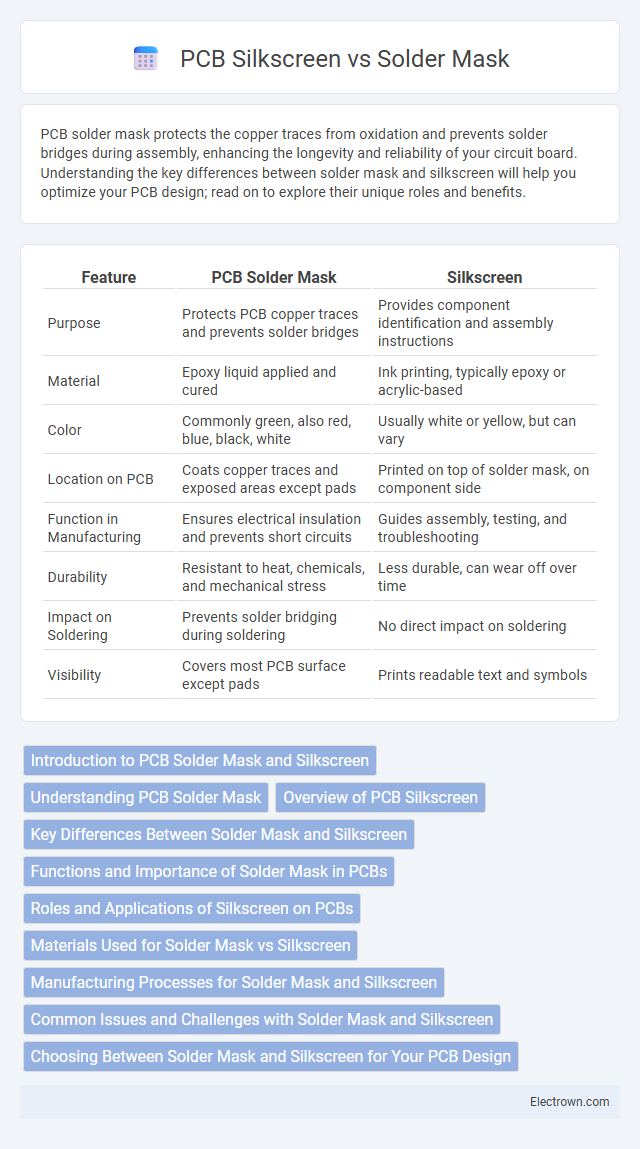
Table of Comparison
| Feature | PCB Solder Mask | Silkscreen |
|---|---|---|
| Purpose | Protects PCB copper traces and prevents solder bridges | Provides component identification and assembly instructions |
| Material | Epoxy liquid applied and cured | Ink printing, typically epoxy or acrylic-based |
| Color | Commonly green, also red, blue, black, white | Usually white or yellow, but can vary |
| Location on PCB | Coats copper traces and exposed areas except pads | Printed on top of solder mask, on component side |
| Function in Manufacturing | Ensures electrical insulation and prevents short circuits | Guides assembly, testing, and troubleshooting |
| Durability | Resistant to heat, chemicals, and mechanical stress | Less durable, can wear off over time |
| Impact on Soldering | Prevents solder bridging during soldering | No direct impact on soldering |
| Visibility | Covers most PCB surface except pads | Prints readable text and symbols |
Introduction to PCB Solder Mask and Silkscreen
PCB solder mask serves as a protective layer that prevents oxidation and solder bridging during assembly, ensuring the integrity of your circuit board. The silkscreen, printed on top of the solder mask, provides essential information such as component labels, logos, and part numbers for easy identification and assembly. Understanding the distinct roles of solder mask and silkscreen enhances the reliability and usability of printed circuit boards.
Understanding PCB Solder Mask
PCB solder mask is a protective layer applied over the copper traces to prevent oxidation and short circuits during soldering, ensuring durability and electrical insulation. Unlike silkscreen, which is used for labeling component locations and providing assembly instructions, the solder mask directly influences the manufacturing quality and reliability of your PCB. Proper understanding of solder mask materials and application techniques is crucial for optimizing circuit performance and minimizing defects.
Overview of PCB Silkscreen
PCB silkscreen is a layer of ink applied to the surface of a printed circuit board to provide labels, symbols, and identification marks for components and connections. This layer enhances assembly accuracy and troubleshooting by clearly indicating component placements, test points, and reference designators. Your ability to efficiently assemble and inspect the PCB is improved through the precise and durable markings offered by the silkscreen layer.
Key Differences Between Solder Mask and Silkscreen
Solder mask is a protective polymer layer applied to printed circuit boards (PCBs) that prevents solder bridges and environmental damage by covering the copper traces, while silkscreen consists of printed text and symbols used for component identification and assembly guidance. Solder mask is typically green, but can come in various colors, and it insulates the board, whereas silkscreen is usually white or black and does not affect electrical insulation. The primary functional difference is that solder mask enhances PCB reliability by protecting conductors, whereas silkscreen improves usability and troubleshooting through clear visual markings.
Functions and Importance of Solder Mask in PCBs
The solder mask on PCBs serves as a protective layer that prevents solder bridges and short circuits by insulating copper traces during assembly, ensuring the board's reliability and electrical integrity. Unlike silkscreen, which provides component labels and reference markings for easier assembly and troubleshooting, the solder mask directly impacts the longevity and performance of your PCB by safeguarding against oxidation and environmental damage. Proper application of solder mask enhances manufacturing precision and reduces the likelihood of defects in electronic devices.
Roles and Applications of Silkscreen on PCBs
Silkscreen on PCBs serves as a critical layer for labeling and identification, providing clear markings for component placement, test points, and reference designators. It enhances assembly accuracy and troubleshooting efficiency by visually guiding technicians during manufacturing and repair processes. Your PCBs benefit from silkscreen by improving readability and ensuring proper component alignment without interfering with electrical functionality.
Materials Used for Solder Mask vs Silkscreen
Solder masks are typically made from liquid photoimageable epoxy or polymer-based materials that provide strong insulation and protection from oxidation and short circuits on your PCB. Silkscreens, on the other hand, use epoxy ink or non-conductive ink designed for clear marking of component placements and reference designators. The durability and chemical composition of solder mask materials ensure optimal electrical performance, while silkscreen inks prioritize visibility and readability on PCB surfaces.
Manufacturing Processes for Solder Mask and Silkscreen
The manufacturing process for PCB solder mask involves applying a liquid photoimageable polymer over the copper traces, which is then exposed to UV light through a photomask and developed to create precise protective coatings that prevent solder bridging and oxidation. In contrast, the silkscreen process uses a stencil to print ink onto the PCB surface, marking component locations, reference designators, and logos to facilitate assembly and inspection. Both processes require precise alignment and curing steps, but solder mask application focuses on insulation and protection, while silkscreen emphasizes informative labeling.
Common Issues and Challenges with Solder Mask and Silkscreen
Common issues with PCB solder mask include masking misalignment, resulting in exposed copper pads or solder bridging, and poor adhesion causing peeling or flaking during assembly. Silkscreen challenges often involve smudging, fading, or incomplete printing, which can lead to misidentification of components and assembly errors. Ensuring proper process controls and material compatibility enhances your PCB reliability by minimizing defects related to both solder mask and silkscreen application.
Choosing Between Solder Mask and Silkscreen for Your PCB Design
Choosing between solder mask and silkscreen for your PCB design depends on their distinct functions: solder mask provides a protective layer preventing solder bridges and corrosion, while silkscreen offers valuable visual information such as component labels and markings. Your PCB's functionality and ease of assembly improve by applying a solder mask to avoid shorts, whereas silkscreen enhances troubleshooting and identification during manufacturing. Prioritizing solder mask ensures electrical reliability, whereas silkscreen optimizes clarity and usability throughout your PCB's lifecycle.
PCB solder mask vs silkscreen Infographic