Si substrates offer cost-effective conductivity ideal for general semiconductor applications, whereas SOI substrates provide superior electrical isolation and reduced parasitic capacitance, enhancing performance in high-speed and low-power devices. Discover which substrate best suits your specific semiconductor needs by exploring the detailed comparisons in the rest of this article.
Table of Comparison
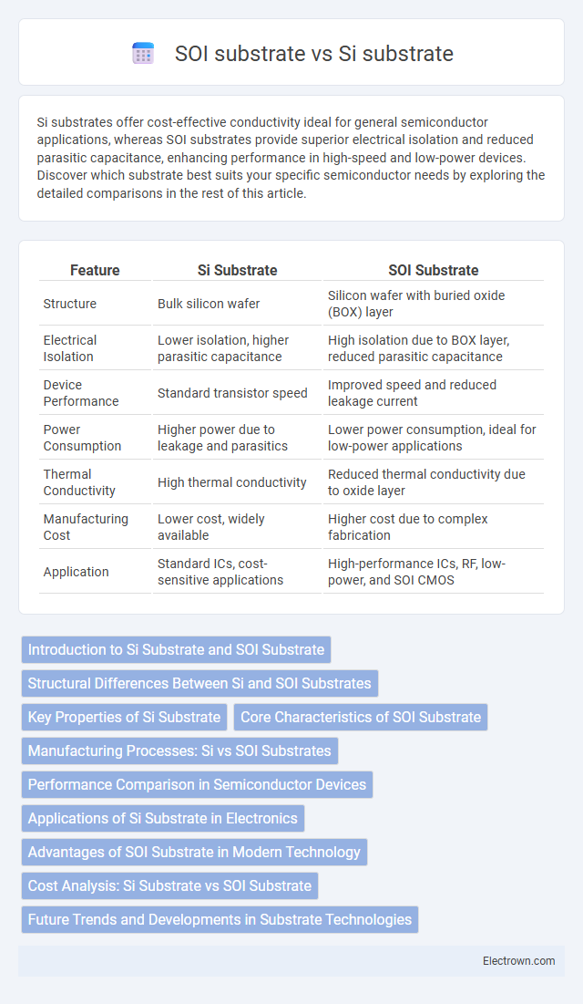
| Feature | Si Substrate | SOI Substrate |
|---|---|---|
| Structure | Bulk silicon wafer | Silicon wafer with buried oxide (BOX) layer |
| Electrical Isolation | Lower isolation, higher parasitic capacitance | High isolation due to BOX layer, reduced parasitic capacitance |
| Device Performance | Standard transistor speed | Improved speed and reduced leakage current |
| Power Consumption | Higher power due to leakage and parasitics | Lower power consumption, ideal for low-power applications |
| Thermal Conductivity | High thermal conductivity | Reduced thermal conductivity due to oxide layer |
| Manufacturing Cost | Lower cost, widely available | Higher cost due to complex fabrication |
| Application | Standard ICs, cost-sensitive applications | High-performance ICs, RF, low-power, and SOI CMOS |
Introduction to Si Substrate and SOI Substrate
Silicon (Si) substrates serve as the foundational base for semiconductor device fabrication, characterized by a uniform crystalline structure that supports integrated circuit formation. Silicon-on-Insulator (SOI) substrates incorporate a thin insulating layer, typically silicon dioxide, between the silicon base wafer and the top silicon layer, enhancing device performance by reducing parasitic capacitance and improving thermal isolation. SOI substrates enable advanced applications such as high-speed, low-power electronics and improved radiation hardness compared to conventional Si substrates.
Structural Differences Between Si and SOI Substrates
Si substrates consist of a single, continuous layer of crystalline silicon, providing a uniform bulk material ideal for conventional semiconductor fabrication. SOI substrates feature a layered structure with a thin silicon device layer separated from the bulk silicon wafer by a buried oxide (BOX) layer, which electrically isolates the device layer and reduces parasitic capacitance. Your choice between Si and SOI substrates depends on the desired electrical isolation, performance enhancements, and device scaling requirements.
Key Properties of Si Substrate
Si substrate features high thermal conductivity and excellent mechanical stability, making it ideal for conventional semiconductor fabrication. Its low cost and mature manufacturing process enable widespread use in microelectronics and MEMS devices. However, Si substrates have higher parasitic capacitance compared to SOI substrates, which can limit device performance in high-speed applications.
Core Characteristics of SOI Substrate
SOI (Silicon-On-Insulator) substrates feature a layered silicon-insulator-silicon structure that significantly reduces parasitic capacitance, enhancing device performance and power efficiency. Compared to traditional Si substrates, SOI offers improved speed, lower power consumption, and better isolation for high-frequency applications. Your designs benefit from reduced short-channel effects and enhanced radiation hardness, making SOI ideal for advanced CMOS technology nodes and specialized electronic devices.
Manufacturing Processes: Si vs SOI Substrates
Silicon (Si) substrates are produced through the Czochralski or Float Zone crystal growth methods, yielding bulk single-crystal wafers optimized for a wide range of semiconductor applications. Silicon-on-Insulator (SOI) substrates involve bonding a thin silicon layer atop an insulating layer, typically silicon dioxide, using techniques such as SIMOX (Separation by IMplantation of OXygen) or wafer bonding with layer transfer. SOI manufacturing offers superior electrical isolation, reduced parasitic capacitance, and enhanced device performance, albeit with higher complexity and cost compared to conventional Si wafer fabrication.
Performance Comparison in Semiconductor Devices
SOI (Silicon-On-Insulator) substrates offer superior device performance compared to traditional Si substrates by reducing parasitic capacitance, which enhances switching speed and lowers power consumption in semiconductor devices. SOI technology improves short-channel effects control, enabling better scalability and higher drive currents for advanced CMOS transistors. While Si substrates are more cost-effective and widely used, SOI wafers enable higher performance in RF, analog, and high-speed digital applications due to their improved isolation and reduced leakage currents.
Applications of Si Substrate in Electronics
Si substrates are extensively used in the fabrication of integrated circuits, power devices, and microelectromechanical systems (MEMS) due to their excellent electrical properties and cost-effectiveness. They provide a reliable foundation for CMOS technology, enabling high-performance processors, sensors, and digital logic circuits in consumer electronics and automotive applications. The widespread use of Si substrates supports mass production and scalability in semiconductor manufacturing, making them essential in everyday electronic devices.
Advantages of SOI Substrate in Modern Technology
SOI (Silicon-On-Insulator) substrates offer significant advantages in modern technology, including reduced parasitic capacitance, which leads to lower power consumption and improved device speed compared to traditional Si (Silicon) substrates. The insulating oxide layer in SOI substrates minimizes leakage currents and enhances radiation hardness, making them ideal for high-performance, low-power applications and aerospace environments. Additionally, SOI technology enables better thermal management and scalability in advanced semiconductor devices, supporting the demands of modern integrated circuits and microelectromechanical systems (MEMS).
Cost Analysis: Si Substrate vs SOI Substrate
Si substrate offers a cost-effective solution for semiconductor manufacturing due to its widespread availability and mature fabrication processes, typically resulting in lower initial material and processing expenses compared to SOI substrate. SOI substrate involves higher costs driven by complex manufacturing techniques such as wafer bonding and thinning, which increase material and processing fees but contribute to performance benefits like reduced parasitic capacitance and improved device isolation. Your choice between Si and SOI substrates should consider the trade-off between higher initial investment for SOI and potential system-level cost savings through enhanced device efficiency and integration.
Future Trends and Developments in Substrate Technologies
Future trends in substrate technologies emphasize enhanced performance and energy efficiency, with SOI (Silicon-On-Insulator) substrates gaining traction due to their superior electrical isolation and reduced parasitic capacitance compared to traditional Si substrates. SOI substrates enable lower power consumption and improved speed, making them ideal for next-generation high-frequency and low-voltage devices. Your choice between Si and SOI substrates will increasingly hinge on application-specific demands for scalability and integration in advanced semiconductor manufacturing.
Si substrate vs SOI substrate Infographic