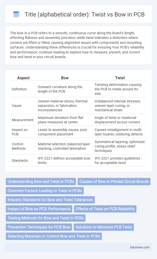
The bow in a PCB refers to a smooth, continuous curve along the board's length, affecting flatness and assembly precision, while twist indicates a distortion where corners are lifted or tilted, causing alignment issues with components and mounting surfaces. Understanding these differences is crucial for ensuring Your PCB's reliability and performance; continue reading to explore how to measure, prevent, and correct bow and twist in your circuit boards.
Table of Comparison
| Aspect | Bow | Twist |
|---|---|---|
| Definition | Outward curvature along the length of the PCB | Twisting deformation causing the PCB to rotate around its axis |
| Cause | Uneven material stress, thermal expansion, or fabrication inconsistencies | Imbalanced internal stresses, uneven layer curing, or mechanical strain |
| Measurement | Maximum deviation from flat plane measured at center | Angle of twist or rotational displacement across corners |
| Impact on PCB | Leads to assembly issues, poor component placement | Causes misalignment in multi-layer boards, soldering defects |
| Control Methods | Material selection, balanced layer stacking, controlled lamination | Symmetrical layering, optimized curing profile, stress relief techniques |
| Standards | IPC-2221 defines acceptable bow limits | IPC-2221 provides guidelines for acceptable twist |
Understanding Bow and Twist in PCBs
Bow and twist are critical mechanical distortions in PCBs that impact board flatness and reliability during assembly. Bow refers to the PCB bending along its length or width, while twist involves warping with one corner lifted compared to the opposite corner, causing uneven surfaces. Understanding these deformations helps you ensure precise component placement and avoid soldering defects in high-quality electronics manufacturing.
Causes of Bow in Printed Circuit Boards
Bow in printed circuit boards primarily results from residual stress caused by uneven cooling rates during the lamination process, leading to dimensional distortion. Variations in material properties, such as differences in the coefficient of thermal expansion between copper layers and substrate, exacerbate this warping effect. Improper layer stacking sequence and asymmetric copper distribution further contribute to bow formation by creating internal mechanical imbalances.
Common Factors Leading to Twist in PCBs
Twist in PCBs often results from uneven thermal expansion during the lamination process, caused by inconsistent material properties or improper cooling rates. Factors such as asymmetric copper distribution, residual stress between layers, and moisture absorption in the substrate contribute significantly to PCB distortion. Managing these variables is crucial to minimizing deformation and ensuring Your boards meet strict flatness specifications.
Industry Standards for Bow and Twist Tolerances
Industry standards for bow and twist tolerances in PCBs are critical to ensure mechanical reliability and performance in electronic assemblies. IPC-A-600 specifies maximum allowable bow and twist limits, typically set at 0.75% of the PCB length, to maintain dimensional stability. Meeting these tolerances minimizes assembly issues, enhances solder joint integrity, and aligns with industry quality control benchmarks.
Impact of Bow on PCB Performance
Bow in PCBs causes uneven surface and dimensional instability, leading to poor solder joint reliability and difficulties during assembly. This warping can result in signal integrity issues and increased mechanical stress, affecting overall device performance and lifespan. Your PCB's functionality and reliability are compromised if bow is not adequately controlled during manufacturing.
Effects of Twist on PCB Reliability
Twist in PCBs introduces mechanical stress that can lead to microcracks in solder joints and delamination of PCB layers, significantly reducing the board's reliability over time. This distortion affects component alignment, causing intermittent electrical connections and signal integrity issues critical in high-frequency applications. Excessive twist can accelerate thermal cycling failures, compromising the long-term durability and performance of electronic devices.
Testing Methods for Bow and Twist in PCBs
Testing methods for bow and twist in PCBs primarily include using optical flatness measurement tools and coordinate measuring machines (CMM) to precisely capture the board's surface deviations. Laser scanners and profilometers provide high-resolution data by scanning the PCB surface to detect warpage and deformation patterns. Mechanical gauges combined with visual inspection are also employed for quick, qualitative assessments of bow and twist during production quality control.
Prevention Techniques for PCB Bow
Preventing PCB bow involves optimizing the lamination process by controlling pre-preg and copper weight distribution to ensure uniform stress across the board. Selecting materials with closely matched coefficients of thermal expansion (CTE) minimizes differential expansion during thermal cycles, reducing bow risk. Implementing gradual cooling profiles and maintaining consistent panel thickness further enhance dimensional stability and prevent bowing in PCBs.
Solutions to Minimize PCB Twist
Minimizing PCB twist involves controlling material selection, layer stacking, and thermal management during manufacturing. Using low CTE (Coefficient of Thermal Expansion) substrates, symmetric layer stacking, and balanced copper distribution reduces internal stresses that cause twisting. Precision in lamination pressure, temperature uniformity, and post-fabrication curing also play critical roles in ensuring flat, twist-free printed circuit boards.
Selecting Materials to Control Bow and Twist in PCBs
Selecting high-Tg FR4 substrates and low CTE prepregs effectively minimizes bow and twist in PCBs by reducing thermal expansion mismatches during manufacturing. Using materials with matched coefficients of thermal expansion ensures uniform stress distribution across PCB layers, maintaining dimensional stability. Implementing materials with controlled resin content and fiber orientation further enhances mechanical integrity, preventing warpage in complex multilayer boards.
Bow vs Twist in PCB Infographic