Tab bonding uses wire connections to attach silicon chips to a substrate, offering simplicity and cost-effectiveness for lower frequency applications, whereas flip chip mounts the chip face-down with solder bumps, enabling superior electrical performance and heat dissipation. Discover which technology best suits your device's needs by reading the full article.
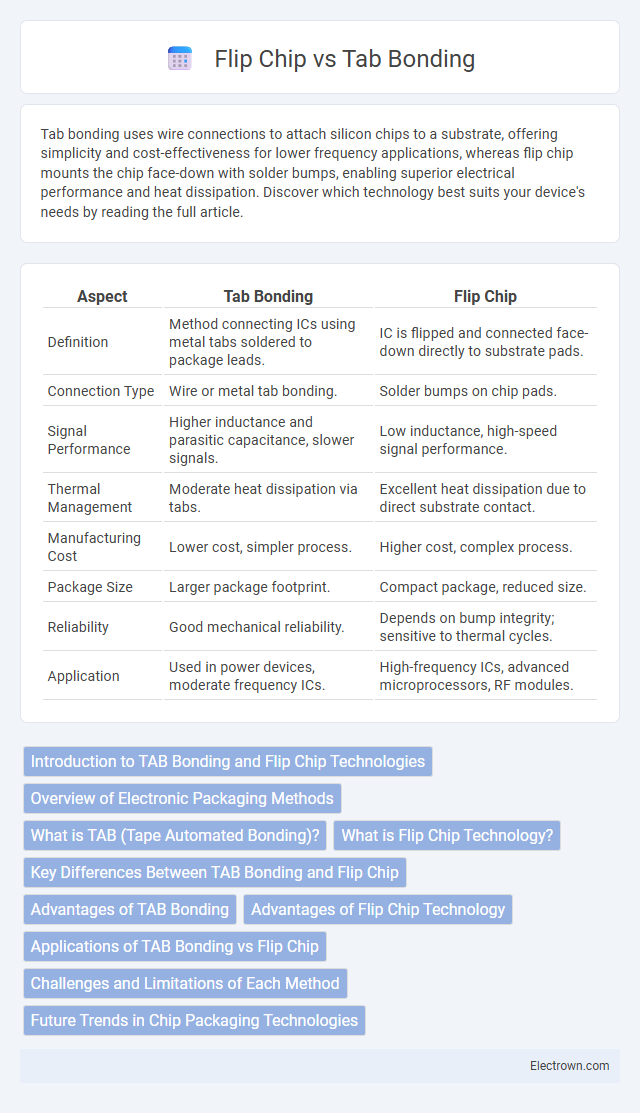
Table of Comparison
| Aspect | Tab Bonding | Flip Chip |
|---|---|---|
| Definition | Method connecting ICs using metal tabs soldered to package leads. | IC is flipped and connected face-down directly to substrate pads. |
| Connection Type | Wire or metal tab bonding. | Solder bumps on chip pads. |
| Signal Performance | Higher inductance and parasitic capacitance, slower signals. | Low inductance, high-speed signal performance. |
| Thermal Management | Moderate heat dissipation via tabs. | Excellent heat dissipation due to direct substrate contact. |
| Manufacturing Cost | Lower cost, simpler process. | Higher cost, complex process. |
| Package Size | Larger package footprint. | Compact package, reduced size. |
| Reliability | Good mechanical reliability. | Depends on bump integrity; sensitive to thermal cycles. |
| Application | Used in power devices, moderate frequency ICs. | High-frequency ICs, advanced microprocessors, RF modules. |
Introduction to TAB Bonding and Flip Chip Technologies
TAB bonding utilizes a thin tape with pre-patterned copper leads to connect semiconductor chips to substrates, offering precise alignment and high-density interconnections ideal for fine-pitch applications. Flip chip technology involves directly flipping the semiconductor die to mount onto a substrate using solder bumps, enabling shorter electrical paths, improved performance, and enhanced heat dissipation. Both methods serve advanced packaging needs but differ in assembly processes, electrical characteristics, and mechanical robustness.
Overview of Electronic Packaging Methods
Tab bonding involves attaching chips to substrates using metal tabs, offering reliable electrical connections with simpler manufacturing processes and lower costs suitable for power devices. Flip chip packaging directly mounts the die face-down onto the substrate, enabling shorter interconnects, higher electrical performance, and better thermal management for high-frequency and miniaturized electronics. Both methods play crucial roles in electronic packaging, balancing factors like thermal conductivity, signal integrity, and assembly complexity depending on application requirements.
What is TAB (Tape Automated Bonding)?
Tape Automated Bonding (TAB) is a semiconductor packaging technology that connects integrated circuits (ICs) to substrates using a flexible tape with pre-patterned copper leads. Unlike flip chip bonding, which uses solder bumps directly on the die's surface, TAB employs fine metal leads on a polyimide tape to create precise electrical connections, enhancing reliability in high-density packaging. This method offers advantages in controlling lead geometry and minimizing thermal stresses during assembly.
What is Flip Chip Technology?
Flip chip technology is a semiconductor packaging method where the die is mounted face-down on the substrate, allowing direct electrical connections through solder bumps. This technique enhances signal transmission speed and thermal performance compared to traditional tab bonding, which uses wire connections. Your designs benefit from flip chip's compact size, increased reliability, and superior electrical efficiency in high-frequency applications.
Key Differences Between TAB Bonding and Flip Chip
TAB bonding uses flexible tape carriers with pre-patterned leads to connect semiconductor chips, enabling fine-pitch interconnections and better mechanical flexibility. Flip chip technology directly attaches the chip face-down onto the substrate using solder bumps, offering improved electrical performance and higher input/output density. Your choice between TAB bonding and flip chip depends on application requirements like signal integrity, thermal management, and assembly complexity.
Advantages of TAB Bonding
TAB bonding offers precise alignment and high-density interconnections, making it ideal for complex integrated circuits with fine pitch requirements. It provides excellent thermal and electrical performance due to its thin, flexible tape substrate, enhancing reliability and signal integrity. Your electronics benefit from reduced package size and improved mechanical stability compared to traditional flip chip methods.
Advantages of Flip Chip Technology
Flip chip technology offers superior electrical performance due to shorter interconnects, resulting in lower inductance and resistance compared to tab bonding. It enables higher input/output (I/O) density, allowing more connections in a smaller footprint, which is critical for advanced integrated circuits. Enhanced thermal management is also a key advantage, as flip chip enables efficient heat dissipation directly through the silicon die to the package substrate.
Applications of TAB Bonding vs Flip Chip
TAB bonding is widely used in applications requiring high-density interconnections and precise alignment, such as LCD displays and automotive electronics, where long, flexible leads are beneficial. Flip chip technology suits high-performance computing and mobile devices, offering superior electrical performance and heat dissipation by directly connecting the chip to the substrate. Your choice depends on factors like device complexity, space constraints, and thermal management needs.
Challenges and Limitations of Each Method
Tab bonding faces challenges such as limited interconnect density and increased inductance, which can affect high-frequency performance. Flip chip offers higher interconnect density and better electrical performance but requires complex under-bump metallization and precise alignment, increasing manufacturing costs. Your choice depends on balancing these trade-offs with application-specific requirements and cost constraints.
Future Trends in Chip Packaging Technologies
Tab bonding and flip chip technologies are pivotal in advancing chip packaging, with flip chip offering superior electrical performance and miniaturization, crucial for next-generation devices. Future trends emphasize enhanced thermal management and high-density interconnects, where flip chip's direct die-to-substrate connection supports higher I/O counts and signal integrity. Your designs will benefit from the evolving integration of these methods with 3D packaging and heterogeneous integration to meet escalating performance and space efficiency demands.
Tab bonding vs Flip chip Infographic