Hard masks provide a rigid, durable barrier ideal for precise etching and high-resolution patterning, while soft masks offer flexibility and better conformal coverage for complex surfaces. Explore the differences further to determine which mask best suits your fabrication needs and enhances your manufacturing process.
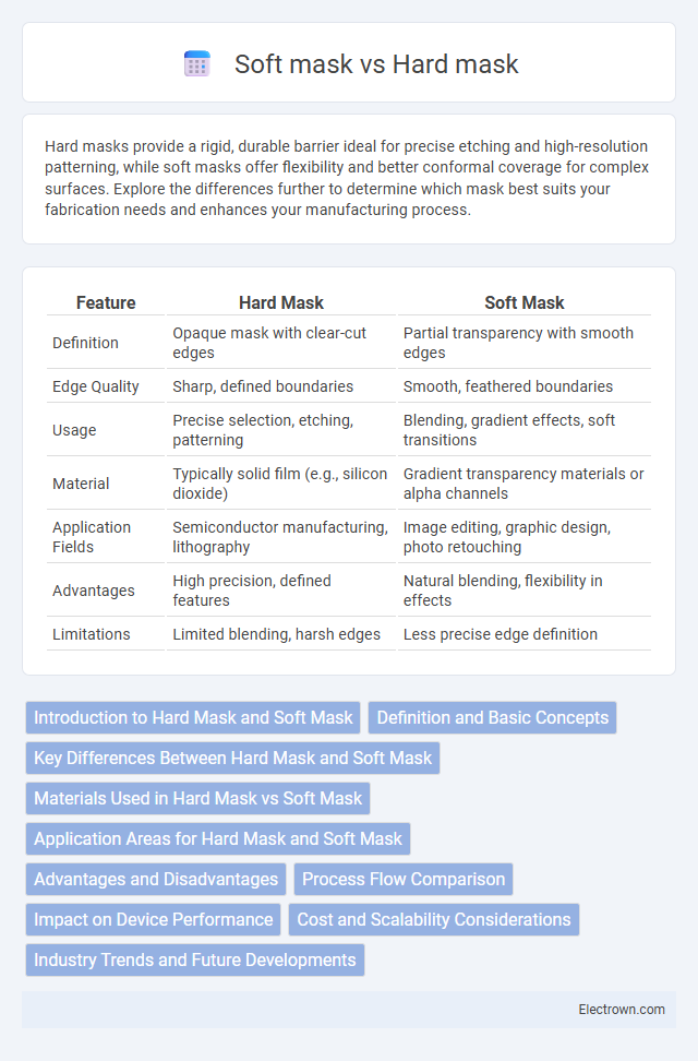
Table of Comparison
| Feature | Hard Mask | Soft Mask |
|---|---|---|
| Definition | Opaque mask with clear-cut edges | Partial transparency with smooth edges |
| Edge Quality | Sharp, defined boundaries | Smooth, feathered boundaries |
| Usage | Precise selection, etching, patterning | Blending, gradient effects, soft transitions |
| Material | Typically solid film (e.g., silicon dioxide) | Gradient transparency materials or alpha channels |
| Application Fields | Semiconductor manufacturing, lithography | Image editing, graphic design, photo retouching |
| Advantages | High precision, defined features | Natural blending, flexibility in effects |
| Limitations | Limited blending, harsh edges | Less precise edge definition |
Introduction to Hard Mask and Soft Mask
Hard mask and soft mask serve as crucial layers in semiconductor fabrication, where a hard mask consists of durable materials like silicon nitride or silicon dioxide that provide high etch resistance and enable precise pattern transfer. Soft masks, typically made from photoresist or polymer materials, offer flexibility in pattern definition but have lower etch resistance and are generally used for less aggressive etching processes. The choice between hard and soft masks depends on factors such as etch selectivity, feature size, and process complexity in microfabrication workflows.
Definition and Basic Concepts
Hard mask refers to a durable, inorganic material like silicon dioxide or silicon nitride used in semiconductor fabrication to protect underlying layers during etching, providing high etch resistance and pattern fidelity. Soft mask consists of organic photoresist materials that are easier to pattern but offer lower etch resistance and are typically used for less aggressive etching processes. The choice between hard mask and soft mask depends on factors such as etch selectivity, pattern complexity, and the desired resolution in microfabrication.
Key Differences Between Hard Mask and Soft Mask
Hard masks are typically composed of materials like silicon nitride or silicon dioxide, offering superior etch resistance and dimensional stability during semiconductor manufacturing. Soft masks, often made from photoresist, provide easier pattern transfer but are more susceptible to damage and deformation due to lower thermal and chemical durability. Understanding these key differences helps optimize your lithography process for precision and efficiency in microfabrication.
Materials Used in Hard Mask vs Soft Mask
Hard masks commonly utilize materials such as silicon nitride (Si3N4), silicon dioxide (SiO2), and metals like chromium or tungsten, which provide high etch resistance and durability during semiconductor fabrication. Soft masks often consist of organic polymers, including photoresists and poly(methyl methacrylate) (PMMA), offering easy patterning but lower etch selectivity compared to hard masks. The choice between hard and soft mask materials significantly impacts pattern fidelity, etch profile, and overall device performance in microfabrication processes.
Application Areas for Hard Mask and Soft Mask
Hard masks are primarily used in semiconductor manufacturing for high-precision patterning in applications such as photolithography and etching, thanks to their durability and resistance to plasma etching. Soft masks find applications in less demanding processes like microfabrication and thin-film patterning, where flexibility and easier removal are preferred. Your choice between hard mask and soft mask depends on the specific requirements of etch selectivity and pattern fidelity in your application area.
Advantages and Disadvantages
Hard masks offer superior etch resistance and dimensional control, making them ideal for high-precision semiconductor fabrication processes. Soft masks provide greater flexibility and easier pattern transfer but suffer from lower durability and potential deformation under aggressive etching conditions. Choosing between hard and soft masks depends on specific process requirements, with hard masks favored for fine features and soft masks suitable for less demanding patterning tasks.
Process Flow Comparison
Hard mask process flow involves depositing a dense, inorganic layer such as silicon nitride or silicon dioxide, patterning it via photolithography, and using it as a robust etch barrier during plasma etching of underlying layers. Soft mask process flow relies on organic photoresist materials directly patterned and used as etch masks, which can be faster but less durable, leading to limitations in etch depth and selectivity. Hard masks offer superior etch resistance and profile control, making them optimal for complex or high-aspect-ratio patterning, while soft masks suit simpler, lower-precision applications.
Impact on Device Performance
Hard masks provide superior etch resistance and dimensional control, resulting in more precise pattern transfer and improved device performance, especially in advanced semiconductor fabrication processes. Soft masks, while easier to apply and remove, often lead to increased line edge roughness and pattern distortion, negatively impacting device reliability and electrical characteristics. The choice between hard and soft masks directly affects critical device parameters such as feature uniformity, defect density, and overall yield.
Cost and Scalability Considerations
Hard masks, typically made from materials like silicon nitride or silicon dioxide, are more durable and provide precise patterning but tend to be costlier due to complex fabrication processes and material expenses. Soft masks, often utilizing photoresist materials, offer lower initial costs and greater flexibility but may face limitations in scalability for high-volume or high-precision manufacturing. Your choice should weigh the balance between upfront investment and scalability demands based on production volume and resolution requirements.
Industry Trends and Future Developments
Hard masks, typically composed of materials like silicon dioxide or silicon nitride, are increasingly favored in semiconductor manufacturing due to their superior etch selectivity and durability in advanced lithography processes. Soft masks, made from photoresist polymers, offer greater pattern resolution but face limitations in high-aspect-ratio etching applications, driving research toward hybrid mask technologies that combine hard mask robustness with soft mask flexibility. Future developments focus on enhancing hard mask materials for next-generation extreme ultraviolet (EUV) lithography and integrating machine learning for predictive etch control, reflecting key industry trends toward increased precision and scalability in microfabrication.
Hard mask vs Soft mask Infographic