Open vias provide a direct electrical connection between layers on a printed circuit board (PCB) without any plating or filling, allowing easier inspection and rework, while filled vias are sealed with conductive or non-conductive materials to improve reliability and prevent solder wicking during assembly. Understanding the differences between open and filled vias can help you choose the best option for your PCB design needs, so explore the rest of the article to learn more.
Table of Comparison
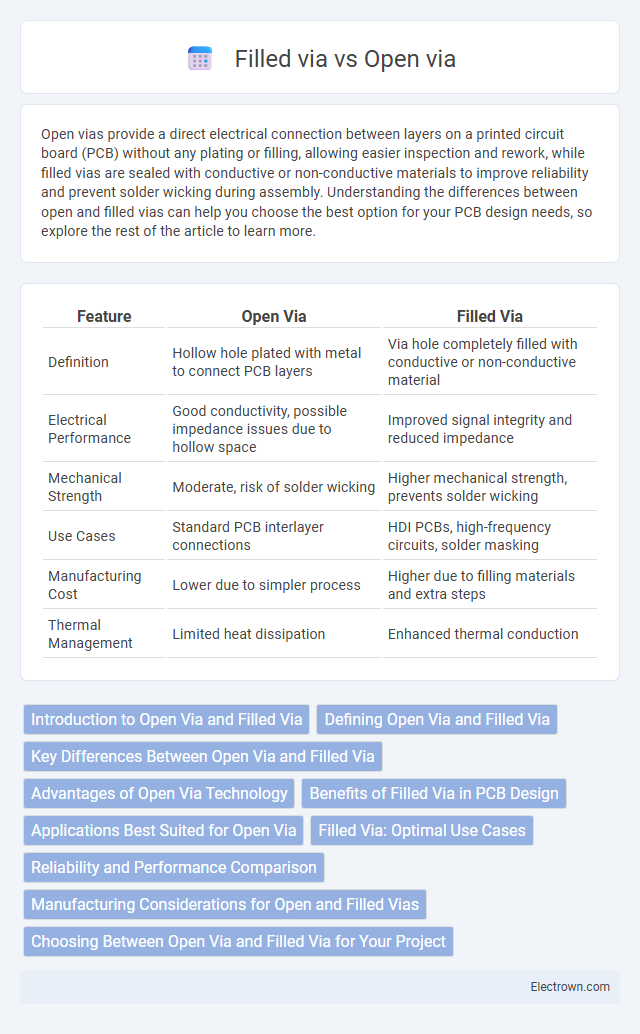
| Feature | Open Via | Filled Via |
|---|---|---|
| Definition | Hollow hole plated with metal to connect PCB layers | Via hole completely filled with conductive or non-conductive material |
| Electrical Performance | Good conductivity, possible impedance issues due to hollow space | Improved signal integrity and reduced impedance |
| Mechanical Strength | Moderate, risk of solder wicking | Higher mechanical strength, prevents solder wicking |
| Use Cases | Standard PCB interlayer connections | HDI PCBs, high-frequency circuits, solder masking |
| Manufacturing Cost | Lower due to simpler process | Higher due to filling materials and extra steps |
| Thermal Management | Limited heat dissipation | Enhanced thermal conduction |
Introduction to Open Via and Filled Via
Open vias are small holes drilled through printed circuit boards (PCBs) that remain unfilled, facilitating electrical connections between layers while reducing manufacturing complexity and cost. Filled vias are similarly drilled holes but are filled with conductive or non-conductive materials like epoxy or copper to enhance structural integrity, improve thermal dissipation, and support surface mount technology in high-density PCBs. Both via types play crucial roles in multilayer PCB design, influencing electrical performance and mechanical reliability.
Defining Open Via and Filled Via
Open vias are plated through-holes in a printed circuit board (PCB) that remain unfilled, providing electrical connectivity between layers while exposing the hole's interior. Filled vias are similar through-holes that are completely filled with conductive or non-conductive material, offering enhanced structural integrity and improved thermal or electrical performance. Your PCB design choice between open and filled vias depends on factors such as manufacturing processes, reliability requirements, and space constraints.
Key Differences Between Open Via and Filled Via
Open vias are small, unfilled holes in a printed circuit board (PCB) that electrically connect different layers and may expose copper, increasing susceptibility to contamination and potential reliability issues. Filled vias are vias completely filled with conductive or non-conductive materials such as epoxy or copper to enhance structural integrity, prevent solder wicking, and improve thermal and electrical performance. The key differences include exposure to environmental elements, mechanical strength, and suitability for high-density PCB applications where reliability and thermal management are critical.
Advantages of Open Via Technology
Open via technology offers superior thermal management by enhancing heat dissipation through its exposed conductive pathways, reducing the risk of overheating in high-power electronic devices. This design facilitates easier inspection and rework during manufacturing, improving overall yield and reliability of printed circuit boards (PCBs). You benefit from improved electrical performance and cost efficiency due to simpler fabrication processes compared to filled via alternatives.
Benefits of Filled Via in PCB Design
Filled vias in PCB design enhance electrical performance by reducing parasitic inductance and capacitance, which improves signal integrity in high-speed circuits. They also provide better mechanical reliability and thermal management by preventing solder wicking and improving heat dissipation. Your designs benefit from increased durability and smoother surface finishes, making filled vias ideal for advanced, high-density applications.
Applications Best Suited for Open Via
Open vias are best suited for high-frequency applications such as RF circuits and microwave PCBs, where signal integrity and minimal parasitic capacitance are critical. They enable effective heat dissipation and easier inspection or rework compared to filled vias. Your designs benefit from open vias when thermal management and electrical performance are prioritized over mechanical strength and planarity.
Filled Via: Optimal Use Cases
Filled vias are ideal for high-frequency and high-speed circuit applications where minimizing signal loss and improving electrical performance is critical. Unlike open vias, filled vias prevent resin entrapment and enhance thermal conductivity, making them suitable for controlled impedance circuits and HDI (High-Density Interconnect) PCBs. Your designs benefit from enhanced reliability and reduced susceptibility to environmental stress when using filled vias in complex multilayer boards.
Reliability and Performance Comparison
Open via structures generally offer greater reliability in high-frequency circuits by minimizing parasitic capacitance and inductance, which leads to better signal integrity and reduced signal loss. Filled via technology, while providing enhanced mechanical strength and lower resistance for thermal dissipation, may introduce slight performance trade-offs due to increased dielectric losses. Your choice between open and filled vias should balance the need for robust electrical performance with mechanical stability depending on the application requirements.
Manufacturing Considerations for Open and Filled Vias
Open vias require precise drilling and plating processes to ensure structural integrity and electrical connectivity, with careful control to avoid defects like copper voids or incomplete plating. Filled vias, often filled with conductive or non-conductive materials, enhance planar surface smoothness, improve thermal management, and support fine-pitch component assembly, but they demand advanced filling technology and additional curing steps. Your manufacturing process must balance cost, reliability, and performance requirements when choosing between open and filled via fabrication techniques.
Choosing Between Open Via and Filled Via for Your Project
Choosing between open via and filled via depends on your project's electrical performance and manufacturing requirements. Open vias offer cost-effective, reliable connections for signal transmission but may cause solder wicking in assembly processes. Filled vias, typically using conductive or non-conductive materials, enhance thermal management and prevent solder migration, making them ideal for high-density or high-reliability PCBs in your design.
open via vs filled via Infographic