Planar inductors offer compact, low-profile designs ideal for high-frequency applications, while wound inductors provide higher inductance values and better energy storage capabilities, making them suitable for power electronics. Discover the key differences and factors to consider when choosing the right inductor for Your specific needs in the rest of the article.
Table of Comparison
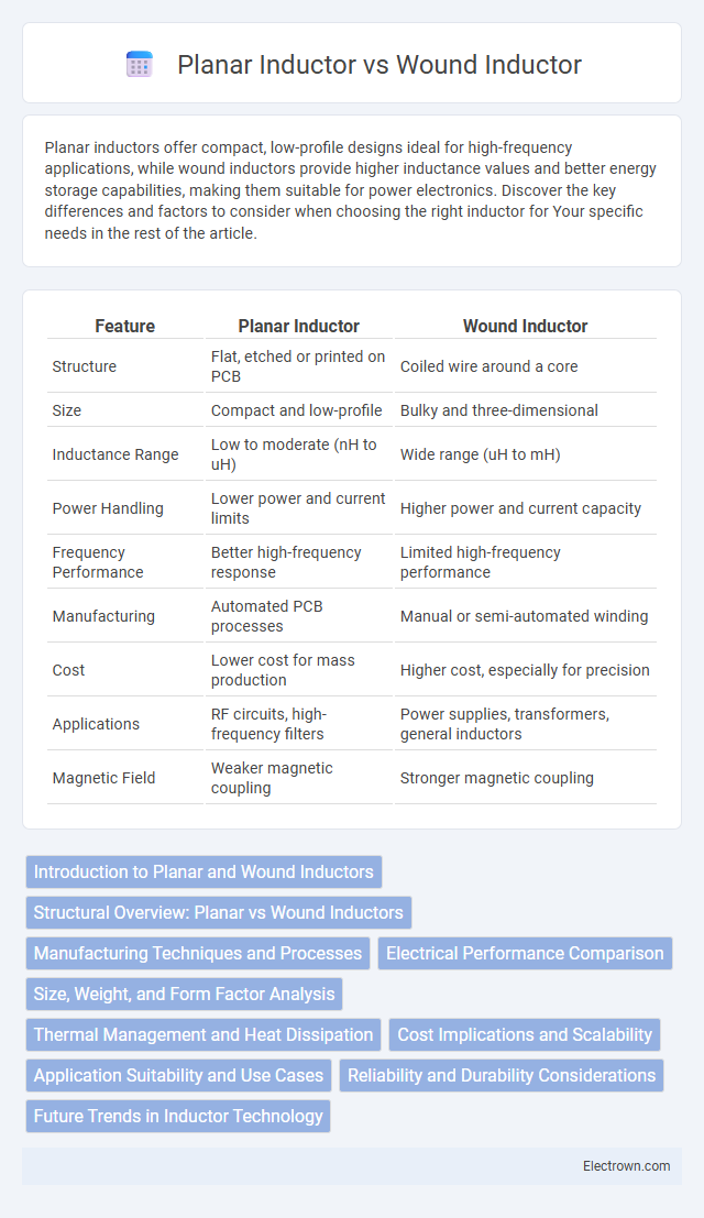
| Feature | Planar Inductor | Wound Inductor |
|---|---|---|
| Structure | Flat, etched or printed on PCB | Coiled wire around a core |
| Size | Compact and low-profile | Bulky and three-dimensional |
| Inductance Range | Low to moderate (nH to uH) | Wide range (uH to mH) |
| Power Handling | Lower power and current limits | Higher power and current capacity |
| Frequency Performance | Better high-frequency response | Limited high-frequency performance |
| Manufacturing | Automated PCB processes | Manual or semi-automated winding |
| Cost | Lower cost for mass production | Higher cost, especially for precision |
| Applications | RF circuits, high-frequency filters | Power supplies, transformers, general inductors |
| Magnetic Field | Weaker magnetic coupling | Stronger magnetic coupling |
Introduction to Planar and Wound Inductors
Planar inductors feature a flat, spiral conductor layout on a printed circuit board, offering compact size and improved thermal management, making them ideal for high-frequency applications. Wound inductors consist of wire coils wrapped around a magnetic core, providing higher inductance and energy storage suitable for power electronics. Your choice between planar and wound inductors depends on space constraints, frequency requirements, and inductance values required for your specific design.
Structural Overview: Planar vs Wound Inductors
Planar inductors feature a flat, spiral-like structure etched onto a printed circuit board, offering compact size and improved thermal management. Wound inductors consist of wire coils wrapped around a core, providing higher inductance values and better magnetic field containment. Your choice depends on space constraints and performance needs, with planar inductors favored for high-frequency applications and wound types for higher current handling.
Manufacturing Techniques and Processes
Planar inductors are typically manufactured using photolithography and thin-film deposition on printed circuit boards (PCBs), allowing for precise geometric control and mass production with high repeatability. Wound inductors use coil winding machines to wrap wire around a core, a process that can be manual or automated but often involves more variability and higher labor costs compared to planar methods. You can achieve smaller form factors and better integration with planar inductors, while wound inductors excel in high inductance and power applications due to their 3D coil structure.
Electrical Performance Comparison
Planar inductors offer lower parasitic capacitance and higher self-resonant frequency compared to wound inductors, resulting in better high-frequency performance and reduced losses. Wound inductors typically exhibit higher inductance values and better current handling due to their three-dimensional coil structure but suffer from increased parasitic effects and lower Q-factor at elevated frequencies. The choice between planar and wound inductors depends on the specific application requirements for frequency response, size constraints, and power handling capabilities.
Size, Weight, and Form Factor Analysis
Planar inductors offer a significantly smaller size and flatter form factor compared to wound inductors, making them ideal for compact circuit designs. Their lightweight structure results from metallic traces patterned on a PCB or substrate, contrasting with the bulkier coil windings of traditional wound inductors. This size and weight advantage facilitates integration into miniaturized electronics where space and mass constraints are critical.
Thermal Management and Heat Dissipation
Planar inductors offer superior thermal management and heat dissipation due to their flat, spread-out design, which increases surface area and enhances cooling efficiency. Wound inductors concentrate heat in a smaller volume, making it harder to dissipate and potentially leading to higher operating temperatures. Optimizing your circuit with planar inductors can improve reliability and performance by maintaining lower thermal resistance and better heat distribution.
Cost Implications and Scalability
Planar inductors generally offer lower manufacturing costs due to their compatibility with standard printed circuit board (PCB) fabrication techniques, making them ideal for high-volume production and easier integration in compact devices. Wound inductors, while more expensive because of their manual or semi-automated assembly and complex materials, provide greater flexibility in inductance values and power handling, which can be beneficial for customized, low-volume applications. Your choice between planar and wound inductors significantly impacts overall cost efficiency and scalability depending on production volume and design requirements.
Application Suitability and Use Cases
Planar inductors excel in high-frequency applications and compact electronic circuits due to their low profile and excellent thermal management, making them ideal for RF modules, power supplies, and integrated circuits. Wound inductors provide higher inductance values and better energy storage capabilities, suitable for power filters, transformers, and low-frequency power conversion systems. Their robustness and tolerance to high current also favor use in automotive electronics and industrial power applications.
Reliability and Durability Considerations
Planar inductors offer enhanced reliability due to their compact, solid-state design, minimizing the risk of mechanical failure and providing superior thermal management compared to traditional wound inductors. Wound inductors, while often offering higher inductance values, are more susceptible to wire fatigue, vibration damage, and insulation breakdown over time. Your choice should consider the specific application's durability requirements, as planar inductors excel in environments demanding long-term stability and resistance to mechanical stress.
Future Trends in Inductor Technology
Future trends in inductor technology emphasize the integration of planar inductors in advanced RF and power applications due to their compact size, lower parasitic capacitance, and ease of fabrication on printed circuit boards. Wound inductors continue to be favored for high-current and high-inductance requirements but face limitations in miniaturization and automated manufacturing. Your choice will increasingly depend on the specific frequency, power, and integration needs as planar inductors become essential in next-generation miniaturized electronic devices.
planar inductor vs wound inductor Infographic