QFN packages offer better thermal performance and electrical characteristics due to their exposed pads and leads, making them ideal for high-frequency applications. Explore the rest of the article to understand how these differences impact your device design and which package suits your needs best.
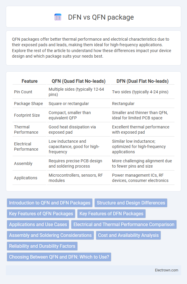
Table of Comparison
| Feature | QFN (Quad Flat No-leads) | DFN (Dual Flat No-leads) |
|---|---|---|
| Pin Count | Multiple sides (typically 12-64 pins) | Two sides (typically 4-24 pins) |
| Package Shape | Square or rectangular | Rectangular |
| Footprint Size | Compact, smaller than equivalent QFP | Smaller and thinner than QFN, ideal for limited PCB space |
| Thermal Performance | Good heat dissipation via exposed pad | Excellent thermal performance with exposed pad |
| Electrical Performance | Low inductance and capacitance, good for high-frequency | Similar low inductance; optimized for high-frequency applications |
| Assembly | Requires precise PCB design and soldering process | More challenging alignment due to fewer pins and size |
| Applications | Microcontrollers, sensors, RF modules | Power management ICs, RF devices, consumer electronics |
Introduction to QFN and DFN Packages
QFN (Quad Flat No-Lead) and DFN (Dual Flat No-Lead) packages are semiconductor surface-mount technologies designed for efficient heat dissipation and space-saving on printed circuit boards. QFN packages feature leads on all four sides, providing enhanced electrical performance and thermal management, while DFN packages have leads on two sides, offering a smaller footprint suitable for compact applications. Both packages improve electrical performance through short lead lengths and low inductance, making them ideal for high-frequency devices.
Structure and Design Differences
QFN (Quad Flat No-lead) packages feature a square or rectangular body with exposed pads on the bottom and leads located beneath the device, which improve heat dissipation and electrical performance. DFN (Dual Flat No-lead) packages have a similar leadframe design but with leads only on two sides, making them more compact and suitable for space-constrained applications. Understanding these structural and design differences helps optimize your PCB layout for better thermal management and signal integrity.
Key Features of QFN Packages
QFN (Quad Flat No-Lead) packages feature a low-profile, square or rectangular body with exposed pads on the underside for improved thermal and electrical performance. Their leadless design enhances board space efficiency while ensuring superior heat dissipation through exposed copper pads connected to the PCB. You benefit from reduced parasitic inductance and enhanced signal integrity, making QFN ideal for high-frequency and compact electronics applications.
Key Features of DFN Packages
DFN (Dual Flat No-lead) packages offer a compact, leadless design that enhances thermal performance and electrical efficiency for high-frequency applications. Their exposed pad allows for improved heat dissipation, making them ideal for power management and RF devices. The flat, no-lead construction facilitates automated PCB assembly and reduces parasitic inductance compared to traditional leaded packages.
Applications and Use Cases
QFN (Quad Flat No-lead) packages are widely used in high-frequency applications such as RF modules, wireless communication devices, and sensor interfaces due to their excellent thermal performance and reduced parasitic inductance. DFN (Dual Flat No-lead) packages are preferred for compact consumer electronics, power management ICs, and automotive sensors where space-saving and efficient heat dissipation are critical. Both packages excel in applications requiring robust mechanical stability and electrical performance in compact form factors.
Electrical and Thermal Performance Comparison
QFN (Quad Flat No-Lead) packages offer superior thermal performance due to their exposed thermal pad, which enhances heat dissipation compared to DFN (Dual Flat No-Lead) packages that generally have smaller pads. Electrically, QFN packages provide lower parasitic inductance and resistance, improving signal integrity and power delivery, especially in high-frequency applications. DFN packages, while compact, may exhibit higher thermal resistance and slightly increased electrical parasitics, making QFN more advantageous for demanding thermal and electrical performance requirements.
Assembly and Soldering Considerations
QFN (Quad Flat No-Lead) packages require precise solder paste application and controlled reflow profiles to ensure reliable solder joint formation under the package pads, minimizing voids and tombstoning risks during assembly. DFN (Dual Flat No-Lead) packages, with fewer pins, offer easier solder mask design and reduced solder bridging potential but demand careful pad design and stencil thickness to achieve consistent solder volume. Your PCB layout should account for thermal relief and pad finishes to optimize heat dissipation and solder joint reliability for both QFN and DFN packages.
Cost and Availability Analysis
QFN (Quad Flat No-lead) packages generally offer lower manufacturing costs due to simpler lead frame designs and higher yield rates compared to DFN (Dual Flat No-lead) packages, which can be more expensive because of their dual-row contacts and complex assembly processes. QFN packages benefit from greater market availability, supported by a wider range of suppliers and standardized footprints, making them easier to source for high-volume production. DFN packages are often limited in availability and tend to be reserved for specialized applications where size constraints outweigh cost considerations.
Reliability and Durability Factors
QFN (Quad Flat No-lead) packages generally offer superior reliability and durability due to their exposed thermal pad, which improves heat dissipation and reduces thermal stress during operation. DFN (Dual Flat No-lead) packages have a smaller footprint but often face challenges with mechanical stress on solder joints, impacting long-term durability under thermal cycling. The choice between QFN and DFN impacts lifecycle performance, with QFN favored in high-reliability automotive and industrial applications due to enhanced mechanical stability and thermal management.
Choosing Between QFN and DFN: Which to Use?
Choosing between QFN (Quad Flat No-Lead) and DFN (Dual Flat No-Lead) packages depends on your PCB space constraints and thermal performance requirements. QFN packages are ideal for applications demanding superior heat dissipation and increased pin count due to their larger footprint and exposed pad design, whereas DFN packages offer a smaller footprint suitable for compact devices with fewer pins. Evaluating your device's power needs and layout flexibility helps determine which package optimizes performance and reliability.
QFN vs DFN package Infographic