Bump bonding offers higher interconnect density and better electrical performance compared to wire bonding, making it ideal for advanced microelectronics applications. Explore this article to understand the differences and determine which bonding technique best suits your electronic packaging needs.
Table of Comparison
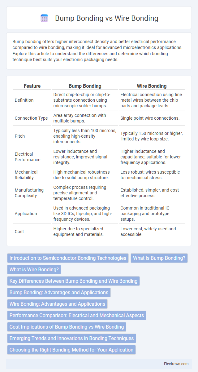
| Feature | Bump Bonding | Wire Bonding |
|---|---|---|
| Definition | Direct chip-to-chip or chip-to-substrate connection using microscopic solder bumps. | Electrical connection using fine metal wires between the chip pads and package leads. |
| Connection Type | Area array connection with multiple bumps. | Single point wire connections. |
| Pitch | Typically less than 100 microns, enabling high-density interconnects. | Typically 150 microns or higher, limited by wire loop size. |
| Electrical Performance | Lower inductance and resistance, improved signal integrity. | Higher inductance and capacitance, suitable for lower frequency applications. |
| Mechanical Reliability | High mechanical robustness due to solid bump structure. | Less robust; wires susceptible to mechanical stress. |
| Manufacturing Complexity | Complex process requiring precise alignment and temperature control. | Established, simpler, and cost-effective process. |
| Application | Used in advanced packaging like 3D ICs, flip-chip, and high-frequency devices. | Common in traditional IC packaging and prototype setups. |
| Cost | Higher due to specialized equipment and materials. | Lower cost, widely used and accessible. |
Introduction to Semiconductor Bonding Technologies
Semiconductor bonding technologies such as bump bonding and wire bonding play critical roles in electrical interconnections within integrated circuits. Bump bonding uses solder or copper bumps to create high-density, low-resistance, and short interconnections, ideal for advanced packaging like 3D ICs and flip-chip modules. Wire bonding involves ultrafine wires, typically gold or aluminum, to connect semiconductor chips to substrates, favored for its cost-effectiveness and flexibility in various packaging applications.
What is Bump Bonding?
Bump bonding is a semiconductor packaging technique that connects a chip to its substrate using tiny solder bumps, enabling high-density interconnections and improved electrical performance. This method allows for shorter signal paths, reduced parasitic inductance, and enhanced thermal conductivity compared to traditional wire bonding. Commonly used in advanced microelectronics, bump bonding supports applications requiring miniaturization and high-speed data transmission, such as in 3D integrated circuits and flip-chip assemblies.
What is Wire Bonding?
Wire bonding is a semiconductor packaging technique that uses fine metal wires, typically gold or aluminum, to establish electrical connections between the chip's bond pads and the package leads. This method is widely utilized due to its cost-effectiveness and compatibility with a variety of semiconductor devices, enabling reliable signal transmission in integrated circuits. Wire bonding is essential in applications where flexible interconnect configurations and proven manufacturing processes are prioritized over higher density connections offered by alternatives like bump bonding.
Key Differences Between Bump Bonding and Wire Bonding
Bump bonding involves creating a direct metallic connection between semiconductor devices using microscopic solder bumps, offering higher density interconnects and better electrical performance compared to wire bonding. Wire bonding connects chips with fine metal wires, typically gold or aluminum, which is more flexible but limits miniaturization and signal integrity. Key differences include bump bonding's suitability for advanced packaging technologies like 3D ICs and flip-chip designs, whereas wire bonding remains preferred for cost-effective, traditional packaging with simpler assembly processes.
Bump Bonding: Advantages and Applications
Bump bonding offers superior electrical performance, higher interconnect density, and reduced parasitic inductance compared to wire bonding, enabling faster signal transmission and improved reliability in advanced semiconductor devices. This technique is widely used in high-frequency applications, 3D integrated circuits, and flip-chip packaging where space constraints and performance are critical. You can leverage bump bonding for enhanced heat dissipation and miniaturized designs, making it ideal for modern microelectronics and high-performance computing systems.
Wire Bonding: Advantages and Applications
Wire bonding offers high flexibility and cost-effectiveness, making it ideal for connecting integrated circuits to package leads in semiconductor manufacturing. Its advantages include compatibility with various substrate materials, suitability for complex chip designs, and ease of automated mass production. Common applications span from microelectronic packaging in consumer electronics to advanced automotive and medical device sensors.
Performance Comparison: Electrical and Mechanical Aspects
Bump bonding offers superior electrical performance due to shorter interconnect lengths, resulting in lower resistance and inductance compared to wire bonding. Mechanically, bump bonds provide enhanced reliability and sturdiness, especially in high-frequency and high-density applications where wire bonds may suffer from wire sweep or fatigue. Your choice between these techniques should consider the specific electrical requirements and mechanical stress conditions of your device to optimize overall performance.
Cost Implications of Bump Bonding vs Wire Bonding
Bump bonding generally incurs higher initial costs than wire bonding due to advanced equipment and complex processing requirements, but it offers superior performance for high-density and high-speed applications. Wire bonding remains cost-effective for low to medium volume production, leveraging simpler machinery and established processes. Long-term cost considerations also favor bump bonding as it enables miniaturization and improved reliability, reducing expenses in compact electronic assemblies.
Emerging Trends and Innovations in Bonding Techniques
Emerging trends in semiconductor packaging highlight the shift from traditional wire bonding to advanced bump bonding techniques, driven by the demand for higher performance and miniaturization in electronics. Innovations such as fine-pitch bump bonding and copper pillar bumps enhance electrical conductivity and thermal management while enabling smaller package footprints. Research into hybrid bonding methods and novel materials continues to improve reliability and integration density, supporting next-generation applications in AI and 5G technology.
Choosing the Right Bonding Method for Your Application
Selecting between bump bonding and wire bonding hinges on factors such as electrical performance, space constraints, and manufacturing complexity. Bump bonding offers superior signal integrity and higher interconnect density, ideal for compact, high-speed applications, whereas wire bonding provides cost-effective flexibility suitable for less space-restricted, lower-frequency designs. Evaluating thermal management needs and production volume is crucial to ensure reliable device assembly and optimal performance.
Bump Bonding vs Wire Bonding Infographic