Source-gated MOSFETs feature a controlled current flow by modulating the source barrier, enhancing device stability and reducing short-channel effects, while drain-gated MOSFETs adjust current via the drain voltage, often impacting output resistance and gain. Explore the detailed comparison to understand which structure best suits your application needs.
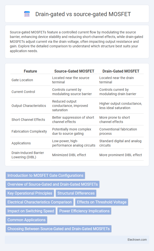
Table of Comparison
| Feature | Source-Gated MOSFET | Drain-Gated MOSFET |
|---|---|---|
| Gate Location | Located near the source terminal | Located near the drain terminal |
| Current Control | Controls current by modulating source barrier | Controls current by modulating drain barrier |
| Output Characteristics | Reduced output conductance, improved saturation | Higher output conductance, less ideal saturation |
| Short Channel Effects | Better suppression of short channel effects | More prone to short channel effects |
| Fabrication Complexity | Potentially more complex due to source gating | Conventional fabrication process |
| Applications | Low-power, high-performance analog circuits | Standard digital and analog circuits |
| Drain-Induced Barrier Lowering (DIBL) | Minimized DIBL effect | More prominent DIBL effect |
Introduction to MOSFET Gate Configurations
MOSFET gate configurations significantly influence device performance, with source-gated and drain-gated architectures representing distinct control schemes. The source-gated MOSFET applies the gate terminal close to the source region, improving channel formation and reducing short-channel effects. In contrast, the drain-gated MOSFET locates the gate near the drain side, affecting the electric field distribution and impact ionization characteristics, which can enhance breakdown voltage but may introduce complexity in device modeling.
Overview of Source-Gated and Drain-Gated MOSFETs
Source-gated MOSFETs control current flow by modulating the potential barrier at the source terminal, which enhances device stability and reduces short-channel effects. Drain-gated MOSFETs, on the other hand, adjust the channel conductivity through the drain potential, often leading to different output characteristics and voltage gain behaviors. Understanding these differences allows you to select the optimal transistor structure for specific analog and digital circuit applications.
Key Operational Principles
Source-gated MOSFETs control current flow by modulating the potential barrier at the source-channel interface, utilizing a depletion region to regulate carrier injection, which enhances saturation characteristics and reduces short-channel effects. Drain-gated MOSFETs primarily modulate current through the electric field at the drain, affecting channel pinch-off and output resistance, typically leading to increased drain-induced barrier lowering (DIBL). The distinct operational principle of source-gated devices offers improved linearity and reduced variability compared to traditional drain-gated MOSFETs, especially in scaled technologies.
Structural Differences
Source-gated MOSFETs feature a control electrode near the source region, which modulates the potential barrier and controls the carrier injection, while drain-gated MOSFETs place the gating influence closer to the drain, affecting the channel conduction primarily near the drain region. The key structural difference lies in the location of the gated electrode: source-gated designs include a depletion region at the source interface for improved current saturation and reduced short-channel effects. Drain-gated structures exhibit conventional channel formation with gate control over the drain-side potential barrier, influencing device behavior mainly under high drain biases.
Electrical Characteristics Comparison
Source-gated MOSFETs exhibit improved control over short-channel effects and reduced drain-induced barrier lowering compared to drain-gated MOSFETs, leading to higher output resistance and better device linearity. Drain-gated MOSFETs typically show faster switching speeds but suffer from increased leakage current and degraded subthreshold slope under high drain bias. Your choice between the two should consider trade-offs in threshold voltage stability, on-state current, and overall device reliability for specific circuit applications.
Effects on Threshold Voltage
Source-gated MOSFETs exhibit a threshold voltage that is less sensitive to drain voltage variations due to the source barrier controlling current flow, enhancing device stability under different operating conditions. Drain-gated MOSFETs, on the other hand, show threshold voltage shifts influenced more significantly by the drain voltage because the channel formation is affected at the drain side. Your circuit design can benefit from source-gated MOSFETs when consistent threshold voltage behavior is critical in varying voltage environments.
Impact on Switching Speed
Source-gated MOSFETs exhibit improved switching speed due to reduced parasitic capacitances at the input node, which enhances the charging and discharging times during signal transitions. Drain-gated MOSFETs often experience slower switching speeds because the gate-drain overlap increases parasitic capacitance, leading to higher delay in the switching process. Optimizing the gate placement relative to the source and drain critically influences the overall device switching performance in high-frequency applications.
Power Efficiency Implications
Source-gated MOSFETs offer improved power efficiency by reducing short-channel effects and minimizing leakage currents compared to drain-gated devices, leading to lower static power consumption. The intrinsic source barrier modulation in source-gated MOSFETs enhances control over the channel, enabling more precise operation at lower voltages and reduced dynamic power loss. Drain-gated MOSFETs typically experience higher power dissipation due to increased drain-induced barrier lowering, which can degrade device performance in low-power applications.
Common Applications
Source-gated MOSFETs are commonly used in low-power circuits and analog signal processing due to their improved control over leakage currents and enhanced linearity. Drain-gated MOSFETs find widespread applications in digital switching circuits and high-frequency amplifiers because of their faster switching speeds and higher gain. Both types are integral in power management systems, with source-gated MOSFETs preferred for energy-efficient designs and drain-gated devices favored in rapid-switching environments.
Choosing Between Source-Gated and Drain-Gated MOSFETs
Choosing between source-gated and drain-gated MOSFETs depends on the specific application requirements involving input impedance, switching speed, and voltage control. Source-gated MOSFETs provide better control over the channel and reduce the device's sensitivity to drain voltage variations, making them ideal for analog circuits and amplifiers. Your selection should balance these characteristics against factors like device complexity and power efficiency to optimize performance in your circuit design.
Source-gated vs drain-gated MOSFET Infographic