Gate-oxide breakdown occurs when the thin insulating layer in a MOS transistor fails due to excessive voltage, causing irreversible damage and leakage currents, while junction breakdown involves the depletion region at a p-n junction collapsing under high reverse bias, leading to a sudden surge in current but without immediate physical damage. Understanding the distinction between these failure modes is crucial for designing reliable semiconductor devices; continue reading to explore their mechanisms, effects, and prevention strategies.
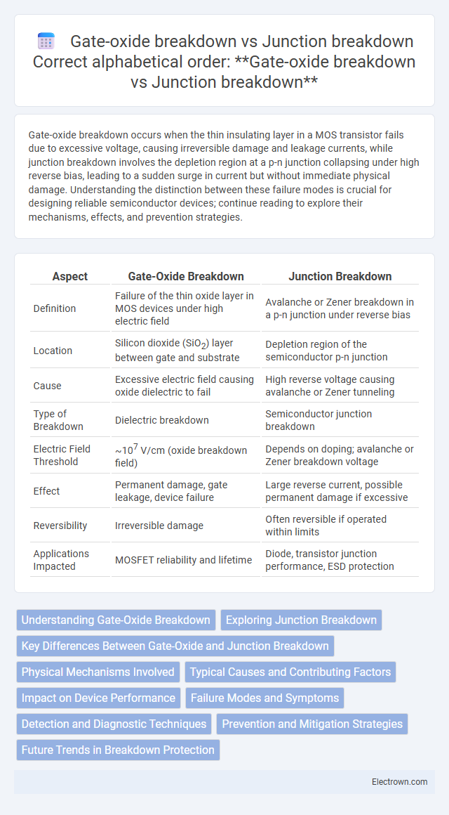
Table of Comparison
| Aspect | Gate-Oxide Breakdown | Junction Breakdown |
|---|---|---|
| Definition | Failure of the thin oxide layer in MOS devices under high electric field | Avalanche or Zener breakdown in a p-n junction under reverse bias |
| Location | Silicon dioxide (SiO2) layer between gate and substrate | Depletion region of the semiconductor p-n junction |
| Cause | Excessive electric field causing oxide dielectric to fail | High reverse voltage causing avalanche or Zener tunneling |
| Type of Breakdown | Dielectric breakdown | Semiconductor junction breakdown |
| Electric Field Threshold | ~107 V/cm (oxide breakdown field) | Depends on doping; avalanche or Zener breakdown voltage |
| Effect | Permanent damage, gate leakage, device failure | Large reverse current, possible permanent damage if excessive |
| Reversibility | Irreversible damage | Often reversible if operated within limits |
| Applications Impacted | MOSFET reliability and lifetime | Diode, transistor junction performance, ESD protection |
Understanding Gate-Oxide Breakdown
Gate-oxide breakdown occurs when the thin insulating layer of silicon dioxide in a MOSFET fails due to excessive electric fields, causing irreversible damage to the device's gate structure. This breakdown mechanism differs from junction breakdown, which involves the depletion region of a semiconductor p-n junction experiencing avalanche or Zener effects under high reverse bias. Understanding gate-oxide breakdown is critical for designing reliable integrated circuits, as it directly impacts transistor performance, leakage currents, and overall device longevity.
Exploring Junction Breakdown
Junction breakdown occurs when the reverse voltage across a p-n junction exceeds a critical level, causing a sudden increase in current due to avalanche or Zener breakdown mechanisms. This phenomenon is critical in semiconductor devices like diodes and transistors because it defines their maximum operating voltage and ensures device reliability. Understanding junction breakdown helps you design circuits that prevent damage from excessive voltage stress, optimizing device performance and longevity.
Key Differences Between Gate-Oxide and Junction Breakdown
Gate-oxide breakdown occurs when the insulating silicon dioxide layer in MOSFETs fails under high electric fields, leading to irreversible damage and leakage currents, while junction breakdown happens at p-n junctions due to high reverse-bias voltage causing avalanche or Zener breakdown. Gate-oxide breakdown is a localized phenomenon associated with thin oxide reliability and tunneling effects, whereas junction breakdown involves space charge region depletion and carrier multiplication mechanisms. The voltage thresholds differ significantly, with gate-oxide breakdown typically occurring at much lower voltages compared to the higher voltages required for junction breakdown.
Physical Mechanisms Involved
Gate-oxide breakdown occurs when the electric field across the thin oxide layer in a MOSFET exceeds its dielectric strength, causing electron tunneling and trap formation that degrade the oxide integrity, ultimately leading to a permanent short circuit. Junction breakdown involves avalanche multiplication or Zener tunneling within the p-n junction depletion region when reverse bias exceeds a critical voltage, resulting in a sudden increase in reverse current. Your device reliability depends on understanding these distinct physical damage mechanisms to prevent catastrophic failure in semiconductor components.
Typical Causes and Contributing Factors
Gate-oxide breakdown typically results from high electric fields causing electron tunneling through the thin oxide layer, often accelerated by defects, impurities, and time-dependent dielectric degradation. Junction breakdown occurs when reverse-biased p-n junctions experience excessive voltage, leading to avalanche multiplication or Zener tunneling, influenced by doping concentration, temperature, and junction geometry. Both breakdown mechanisms are critically impacted by material quality, operational stress, and intrinsic device structures.
Impact on Device Performance
Gate-oxide breakdown causes a severe degradation in transistor switching behavior by introducing leakage currents and reducing gate control, ultimately leading to device failure. Junction breakdown results in excessive current flow through the pn-junction, causing thermal runaway and permanent damage, which compromises overall circuit reliability. Both mechanisms significantly impair device performance, but gate-oxide breakdown primarily affects switching speed and power consumption, whereas junction breakdown impacts current handling and device integrity.
Failure Modes and Symptoms
Gate-oxide breakdown occurs when the thin insulating oxide layer in a MOSFET fails, leading to excessive leakage current and permanent damage to the transistor's switching ability. Junction breakdown takes place when the p-n junction experiences a reverse-bias voltage exceeding its critical limit, causing avalanche or zener breakdown, which results in high current flow and potential device destruction. Your circuits may exhibit symptoms such as increased power dissipation, erratic behavior, or complete failure depending on the breakdown type and severity.
Detection and Diagnostic Techniques
Gate-oxide breakdown detection primarily relies on techniques such as time-dependent dielectric breakdown (TDDB) testing and leakage current monitoring, which identify early signs of oxide degradation through increased current flow or shifts in threshold voltage. Junction breakdown is diagnosed using reverse I-V characterization and electroluminescence imaging to detect avalanche effects and localized leakage paths within the junction region. Advanced diagnostic methods like scanning capacitance microscopy (SCM) and deep-level transient spectroscopy (DLTS) provide detailed analysis of defect states and breakdown mechanisms in both gate oxides and p-n junctions.
Prevention and Mitigation Strategies
Gate-oxide breakdown prevention relies on enhancing the oxide material quality through advanced fabrication techniques such as atomic layer deposition and implementing robust dielectric materials like high-k oxides to improve reliability. Junction breakdown mitigation involves optimizing doping profiles to control electric field distribution, employing guard ring structures, and ensuring proper device scaling to prevent avalanche effects. Both breakdown types benefit from precise voltage and current management during device operation to minimize stress and extend semiconductor lifespan.
Future Trends in Breakdown Protection
Future trends in breakdown protection emphasize advanced materials like high-k dielectrics and wide-bandgap semiconductors to enhance gate-oxide breakdown resistance and junction breakdown voltage. Innovations in transistor design, such as ultra-thin oxide layers and optimized doping profiles, improve device reliability under high electric fields. Your electronic systems will benefit from integrated smart monitoring technologies that predict and mitigate breakdown events before they cause irreversible damage.
Gate-oxide breakdown vs Junction breakdown Infographic