N-well and P-well CMOS technologies differ primarily in the substrate type used for forming transistors: N-well CMOS uses a p-type substrate with n-type wells for PMOS transistors, while P-well CMOS employs an n-type substrate with p-type wells for NMOS transistors. Understanding these distinctions can help you optimize device performance and fabrication processes; continue reading to explore their detailed applications and benefits.
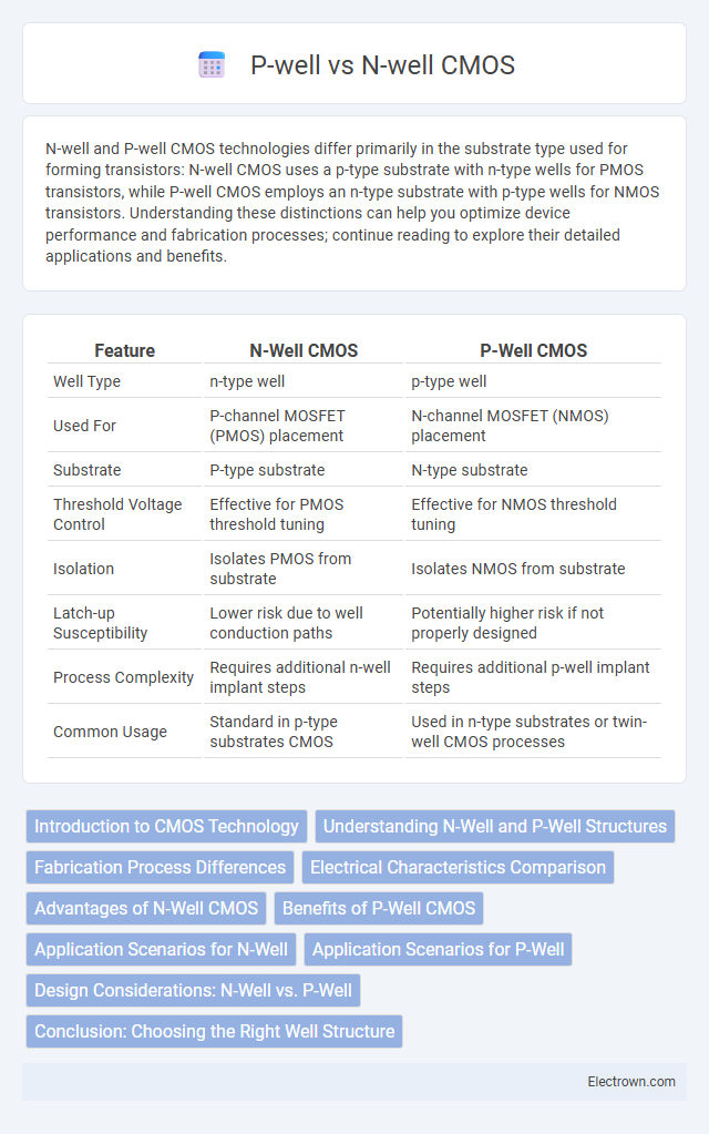
Table of Comparison
| Feature | N-Well CMOS | P-Well CMOS |
|---|---|---|
| Well Type | n-type well | p-type well |
| Used For | P-channel MOSFET (PMOS) placement | N-channel MOSFET (NMOS) placement |
| Substrate | P-type substrate | N-type substrate |
| Threshold Voltage Control | Effective for PMOS threshold tuning | Effective for NMOS threshold tuning |
| Isolation | Isolates PMOS from substrate | Isolates NMOS from substrate |
| Latch-up Susceptibility | Lower risk due to well conduction paths | Potentially higher risk if not properly designed |
| Process Complexity | Requires additional n-well implant steps | Requires additional p-well implant steps |
| Common Usage | Standard in p-type substrates CMOS | Used in n-type substrates or twin-well CMOS processes |
Introduction to CMOS Technology
CMOS technology utilizes complementary n-well and p-well structures to form both NMOS and PMOS transistors on a single silicon substrate, enabling low power consumption and high noise immunity. The n-well houses PMOS transistors by implanting a lightly doped p-type substrate with n-type material, while the p-well contains NMOS transistors within an n-type substrate. Understanding the differences between n-well and p-well layouts is essential for optimizing your integrated circuit design for performance and efficiency.
Understanding N-Well and P-Well Structures
N-Well and P-Well structures form the fundamental building blocks in CMOS technology, where N-Well regions are doped with donor impurities to create electron-rich areas, and P-Well regions are doped with acceptor impurities to create hole-rich areas. N-Wells typically host PMOS transistors, while P-Wells house NMOS transistors, enabling complementary operation with reduced power consumption and improved noise immunity. Precise doping concentration, well depth, and isolation techniques in N-Well and P-Well designs significantly impact transistor threshold voltages, leakage currents, and overall device performance.
Fabrication Process Differences
N-well CMOS fabrication involves creating a deep, heavily doped n-type region in the p-type substrate to house PMOS transistors, while p-well CMOS requires forming p-type wells in an n-type substrate for NMOS devices. The choice between n-well and p-well affects the doping steps, implantation energies, and well formation sequences during the fabrication process. Understanding these differences helps optimize your CMOS design for performance, leakage control, and process compatibility.
Electrical Characteristics Comparison
N-well CMOS technology uses an n-type well in a p-type substrate, offering low leakage currents and high noise immunity suitable for high-speed applications, while p-well CMOS employs a p-type well in an n-type substrate, providing better latch-up resistance and improved threshold voltage control. Electrical characteristics such as body effect, threshold voltage variation, and junction capacitance differ, with n-well CMOS typically displaying stronger coupling between the body and the channel compared to p-well CMOS. Your choice between n-well and p-well CMOS impacts power consumption, switching speed, and overall device reliability depending on the specific circuit requirements.
Advantages of N-Well CMOS
N-Well CMOS technology offers superior noise immunity and better latch-up resistance compared to P-Well CMOS, making it ideal for high-performance and mixed-signal integrated circuits. The N-Well process enables easier integration of PMOS transistors with lower substrate bias sensitivity, enhancing device reliability and reducing leakage currents. These advantages contribute to improved overall power efficiency and faster switching speeds in advanced semiconductor designs.
Benefits of P-Well CMOS
P-well CMOS technology offers enhanced electron mobility compared to N-well, resulting in faster NMOS transistor switching speeds and improved overall device performance. Its compatibility with standard NMOS fabrication steps reduces manufacturing complexity and costs. P-well CMOS also provides better noise immunity and threshold voltage control, making it ideal for low-power, high-speed integrated circuits.
Application Scenarios for N-Well
N-well CMOS technology is predominantly used in standard digital circuits and mixed-signal applications due to its ability to isolate PMOS transistors within an NMOS substrate, enhancing noise immunity and latch-up resistance. Your design can leverage n-well regions to optimize power efficiency and improve transistor performance in high-speed logic circuits and analog components. These properties make n-well CMOS ideal for microprocessors, memory devices, and low-power integrated circuits requiring robust electrical isolation.
Application Scenarios for P-Well
P-well CMOS technology is predominantly utilized in NMOS transistor fabrication due to its positive-type doping, making it suitable for high-speed digital circuits and low-threshold voltage applications. Common application scenarios for p-well include integrated circuits such as microprocessors and memory devices where NMOS performance is critical. Furthermore, p-well integration facilitates complementary CMOS design by allowing n-well formation elsewhere on the substrate, enhancing overall chip functionality and power efficiency.
Design Considerations: N-Well vs. P-Well
N-well and P-well CMOS design considerations primarily involve substrate biasing, latch-up prevention, and device isolation. N-well technology uses a p-type substrate with n-wells for PMOS transistors, offering better control of threshold voltage and noise immunity, whereas P-well employs an n-type substrate with p-wells for NMOS devices, often resulting in faster switching speeds but increased latch-up susceptibility. Your choice between N-well and P-well depends on the required electrical performance, power consumption, and fabrication compatibility for the specific CMOS application.
Conclusion: Choosing the Right Well Structure
Selecting the appropriate well structure in CMOS design depends on your specific circuit requirements and process technology. N-well is typically preferred for PMOS transistors due to its effective isolation and noise immunity, while P-well is suited for NMOS devices, offering advantages in threshold voltage control and reduced latch-up risk. Understanding the trade-offs between n-well and p-well technologies ensures optimized performance, power efficiency, and device reliability in your integrated circuits.
n-well vs p-well CMOS Infographic