The Miller Effect amplifies the effective input capacitance in amplifiers, significantly impacting high-frequency performance, whereas parasitic capacitance refers to unintended capacitances caused by component layout and proximity, which degrade circuit efficiency. Explore the rest of the article to understand how these phenomena affect your circuit design and how to mitigate their effects.
Table of Comparison
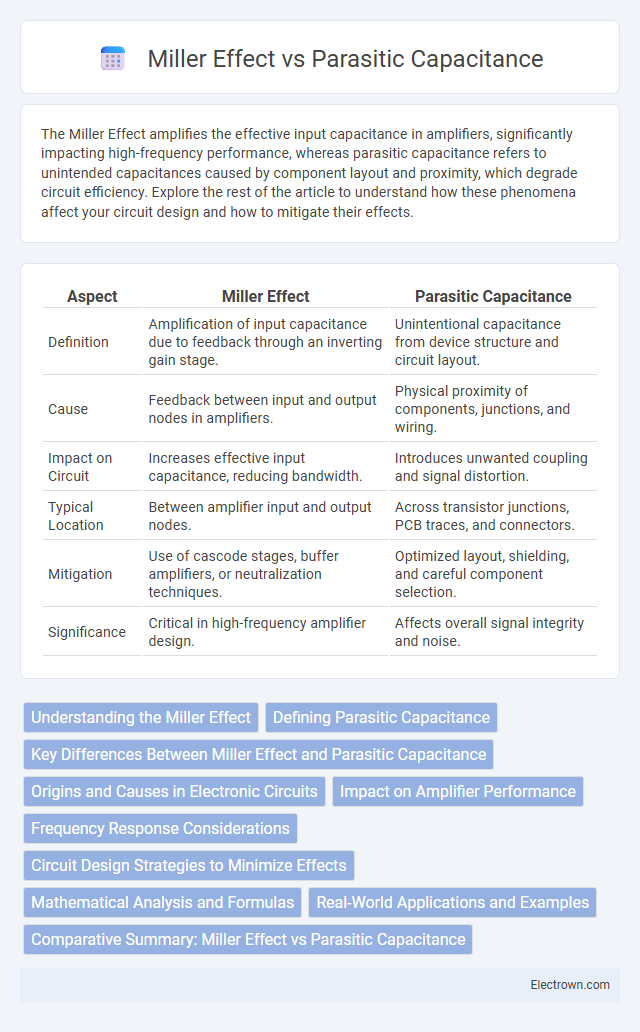
| Aspect | Miller Effect | Parasitic Capacitance |
|---|---|---|
| Definition | Amplification of input capacitance due to feedback through an inverting gain stage. | Unintentional capacitance from device structure and circuit layout. |
| Cause | Feedback between input and output nodes in amplifiers. | Physical proximity of components, junctions, and wiring. |
| Impact on Circuit | Increases effective input capacitance, reducing bandwidth. | Introduces unwanted coupling and signal distortion. |
| Typical Location | Between amplifier input and output nodes. | Across transistor junctions, PCB traces, and connectors. |
| Mitigation | Use of cascode stages, buffer amplifiers, or neutralization techniques. | Optimized layout, shielding, and careful component selection. |
| Significance | Critical in high-frequency amplifier design. | Affects overall signal integrity and noise. |
Understanding the Miller Effect
The Miller Effect significantly impacts amplifier design by effectively multiplying the parasitic capacitance between the input and output nodes, causing an increase in the equivalent input capacitance and reducing the bandwidth. Parasitic capacitance, inherent in transistor junctions and layout, typically limits high-frequency performance, but the Miller Effect exacerbates this limitation by feedback voltage gain that scales the capacitance. Understanding the Miller Effect is essential for predicting frequency response and implementing compensation techniques in high-gain stages.
Defining Parasitic Capacitance
Parasitic capacitance refers to unintended capacitive coupling between circuit elements, often caused by physical proximity and layout of components within an electronic device. It introduces unwanted charge storage that can degrade circuit performance by affecting frequency response and signal integrity. Understanding parasitic capacitance is crucial for analyzing the Miller Effect, which amplifies the apparent input capacitance in amplifiers due to feedback and can significantly impact high-frequency behavior.
Key Differences Between Miller Effect and Parasitic Capacitance
The Miller Effect refers to the apparent multiplication of an input capacitance caused by feedback through an inverting amplifier stage, significantly impacting high-frequency response in amplifiers. Parasitic Capacitance, on the other hand, consists of unintended capacitances inherent within semiconductor devices and circuit layouts, affecting signal integrity and switching speeds. Unlike general parasitic capacitances, the Miller Effect specifically amplifies capacitance between input and output nodes, often requiring careful compensation in high-gain amplifier designs.
Origins and Causes in Electronic Circuits
The Miller Effect arises from the feedback capacitance between an amplifier's input and output, effectively multiplying this capacitance and impacting high-frequency response. Parasitic capacitance originates from the unintended capacitive coupling between circuit components and conductive traces, often due to device layout and physical proximity. Understanding these causes helps optimize your circuit design to minimize signal degradation and improve overall performance.
Impact on Amplifier Performance
The Miller effect significantly increases the effective input capacitance in amplifiers, causing a reduction in bandwidth and slowing the frequency response, which impedes high-frequency performance. Parasitic capacitance, arising from unintentional capacitances within the circuit layout, contributes to noise and signal degradation, further limiting amplifier gain and stability at high frequencies. Both phenomena critically degrade amplifier performance by introducing unwanted capacitive loading, necessitating careful design considerations to optimize frequency response and maintain signal integrity.
Frequency Response Considerations
Miller effect significantly amplifies parasitic capacitance in high-frequency circuits, causing a decrease in the overall bandwidth and degrading the frequency response of amplifiers. Parasitic capacitance, typically found between transistor terminals, directly impacts the gain-bandwidth product by introducing unwanted feedback paths that limit high-frequency performance. Effective circuit design minimizes the Miller effect by using cascode configurations or neutralization techniques, thereby improving frequency response and signal integrity in RF and analog applications.
Circuit Design Strategies to Minimize Effects
Circuit design strategies to minimize the Miller effect and parasitic capacitance focus on reducing unwanted feedback and signal distortion in high-frequency applications. Techniques include using cascode amplifier configurations, which isolate input and output nodes to lower effective input capacitance, and implementing careful layout practices such as minimizing trace lengths and shielding sensitive nodes to reduce parasitic capacitance. Your design benefits from selecting low-capacitance components and employing buffer stages to preserve signal integrity and enhance circuit performance.
Mathematical Analysis and Formulas
Miller Effect magnifies input capacitance through multiplication by the gain factor, mathematically represented as C_M = C_p (1 - A_v), where C_M is the effective capacitance, C_p is the parasitic capacitance, and A_v is the voltage gain. Parasitic capacitance, often denoted as C_p, exists inherently within transistor junctions and circuit layouts, affecting high-frequency response by introducing unwanted capacitive reactance. Your circuit's frequency response can be precisely analyzed by considering both effects using formulas such as f_H = 1 / (2pR_in(C_in + C_M)) to determine the high-frequency cutoff influenced by Miller capacitance.
Real-World Applications and Examples
In real-world applications, the Miller effect significantly impacts high-frequency amplifier design by increasing the effective input capacitance, often leading to bandwidth limitations. Parasitic capacitance, inherent in all electronic components and circuit layouts, can cause unwanted coupling and signal degradation, affecting circuit performance in RF and high-speed digital systems. Understanding these phenomena helps you optimize circuit stability and improve overall device reliability in practical scenarios such as amplifier stages and integrated circuit design.
Comparative Summary: Miller Effect vs Parasitic Capacitance
The Miller Effect significantly amplifies the input capacitance in amplifiers due to feedback through the gain stage, making it a dominant factor in frequency response degradation. Parasitic capacitance, originating from inherent device structures and interconnects, adds unwanted capacitive loads but usually remains constant regardless of gain. Understanding these distinctions enables you to better manage high-frequency circuit performance by addressing gain-dependent Miller capacitance separately from fixed parasitic values.
Miller Effect vs Parasitic Capacitance Infographic