Wafer level packaging (WLP) integrates the packaging process directly on the wafer, enabling smaller package sizes and improved electrical performance compared to traditional chip scale packaging (CSP), which packages individual chips after dicing. Understanding the benefits and applications of each technology can help you choose the best solution for your semiconductor design--explore the full article for detailed insights.
Table of Comparison
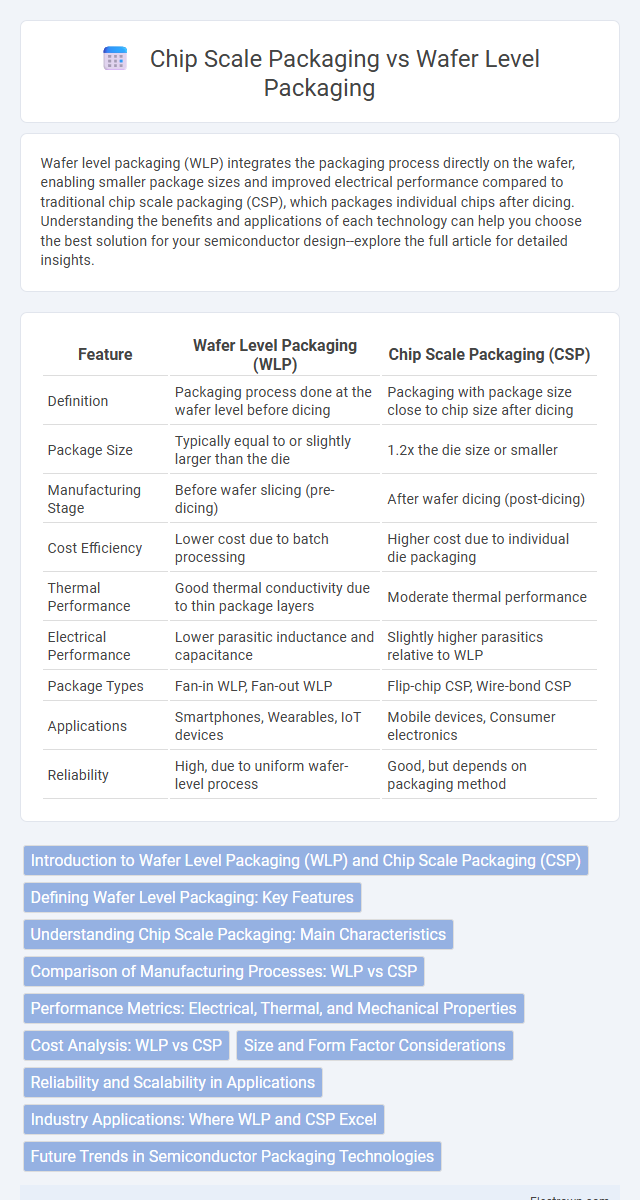
| Feature | Wafer Level Packaging (WLP) | Chip Scale Packaging (CSP) |
|---|---|---|
| Definition | Packaging process done at the wafer level before dicing | Packaging with package size close to chip size after dicing |
| Package Size | Typically equal to or slightly larger than the die | 1.2x the die size or smaller |
| Manufacturing Stage | Before wafer slicing (pre-dicing) | After wafer dicing (post-dicing) |
| Cost Efficiency | Lower cost due to batch processing | Higher cost due to individual die packaging |
| Thermal Performance | Good thermal conductivity due to thin package layers | Moderate thermal performance |
| Electrical Performance | Lower parasitic inductance and capacitance | Slightly higher parasitics relative to WLP |
| Package Types | Fan-in WLP, Fan-out WLP | Flip-chip CSP, Wire-bond CSP |
| Applications | Smartphones, Wearables, IoT devices | Mobile devices, Consumer electronics |
| Reliability | High, due to uniform wafer-level process | Good, but depends on packaging method |
Introduction to Wafer Level Packaging (WLP) and Chip Scale Packaging (CSP)
Wafer Level Packaging (WLP) involves packaging integrated circuits directly at the wafer level, enabling smaller form factors and improved electrical performance by eliminating traditional packaging steps. Chip Scale Packaging (CSP) refers to packaging methods where the package size is nearly the same as the semiconductor die, optimizing space and enhancing thermal and electrical characteristics. Your choice between WLP and CSP impacts device miniaturization, performance efficiency, and manufacturing cost-effectiveness in electronic applications.
Defining Wafer Level Packaging: Key Features
Wafer Level Packaging (WLP) involves packaging integrated circuits directly at the wafer level before dicing, enabling smaller package sizes and improved electrical performance. Key features of WLP include reduced package footprint, enhanced thermal management, and higher input/output (I/O) density compared to traditional Chip Scale Packaging (CSP). WLP supports advanced applications requiring miniaturization and reliable high-frequency performance in smartphones, IoT devices, and wearables.
Understanding Chip Scale Packaging: Main Characteristics
Chip Scale Packaging (CSP) is a type of semiconductor packaging that closely matches the size of the die, typically no more than 20% larger than the chip itself, enabling compact and efficient designs. The main characteristics of CSP include a reduced footprint, enhanced electrical performance due to shorter interconnects, and improved thermal management, which support higher device density on circuit boards. You benefit from faster signal transmission and lower manufacturing costs compared to traditional wafer level packaging methods.
Comparison of Manufacturing Processes: WLP vs CSP
Wafer Level Packaging (WLP) involves packaging at the wafer scale before dicing, enabling simultaneous encapsulation and testing of multiple dies, which enhances throughput and reduces manufacturing complexity. Chip Scale Packaging (CSP) typically encompasses packaging after die singulation, using substrate materials and processes like wire bonding or flip-chip, resulting in larger package footprints compared to WLP. Your choice between WLP and CSP impacts production efficiency, package size, and integration capabilities depending on specific application requirements.
Performance Metrics: Electrical, Thermal, and Mechanical Properties
Wafer Level Packaging (WLP) offers superior electrical performance due to shorter interconnects, which reduce signal inductance and resistance, enhancing high-frequency operation. Thermal management in WLP benefits from its thin profile and direct heat paths, enabling efficient heat dissipation compared to traditional Chip Scale Packaging (CSP). Mechanically, WLP provides better stress distribution and reliability in fine-pitch applications, while CSP delivers robust protection but may suffer from higher mechanical strain due to larger package size and solder joint dimensions.
Cost Analysis: WLP vs CSP
Wafer Level Packaging (WLP) typically offers lower production costs compared to Chip Scale Packaging (CSP) due to its streamlined wafer-level process that reduces material waste and assembly steps. CSP may incur higher costs from additional packaging components and more complex assembly procedures, impacting overall manufacturing expenses. Your choice between WLP and CSP should consider these cost differences alongside performance and application requirements for optimal value.
Size and Form Factor Considerations
Wafer Level Packaging (WLP) offers a smaller and more uniform form factor by packaging chips directly at the wafer level, enabling ultra-compact designs ideal for mobile and wearable devices. Chip Scale Packaging (CSP) maintains a size closely matching the die itself but involves individual die packaging, which can result in slightly larger footprints compared to WLP. The smaller footprint and reduced package thickness of WLP provide superior benefits for high-density integration and miniaturization requirements in advanced electronics.
Reliability and Scalability in Applications
Wafer Level Packaging (WLP) offers superior reliability due to its shorter interconnects and reduced parasitic effects compared to Chip Scale Packaging (CSP), enhancing signal integrity and thermal performance in high-frequency and high-density applications. CSP, while slightly less robust, provides greater scalability and cost advantages for mass production through its standardized package sizes and compatibility with automated assembly processes. Both technologies are critical in advanced electronics, but WLP is preferred for applications demanding higher reliability, whereas CSP excels in scalable, cost-effective solutions.
Industry Applications: Where WLP and CSP Excel
Wafer Level Packaging (WLP) excels in mobile and consumer electronics due to its ultra-thin profile and superior electrical performance, making it ideal for smartphones and wearables that demand compact, high-speed connectivity. Chip Scale Packaging (CSP) is widely used in automotive and industrial applications where reliability and thermal management are critical, supporting robust device operation in harsh environments. Your choice between WLP and CSP depends on specific application needs such as size constraints, performance requirements, and environmental resilience.
Future Trends in Semiconductor Packaging Technologies
Future trends in semiconductor packaging technologies emphasize wafer level packaging (WLP) and chip scale packaging (CSP) due to their scalability and performance enhancements. WLP offers superior electrical performance and thermal management by integrating packaging processes at the wafer level, reducing size and cost for high-density applications. CSP continues to evolve with advancements in materials and fine-pitch interconnects, enabling ultra-compact designs critical for mobile and IoT devices.
Wafer level packaging vs Chip scale packaging Infographic