DRC (Design Rule Checking) ensures your layout complies with foundry-specific geometric and spacing rules to prevent manufacturing defects, while LVS (Layout Versus Schematic) verifies that the layout matches the intended circuit schematic to confirm functional correctness. Understanding the differences between DRC and LVS will help you optimize your chip design process; explore the full article to learn more.
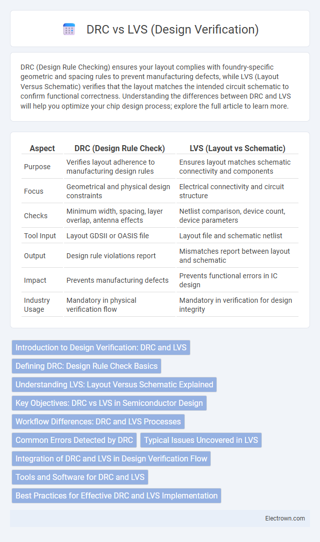
Table of Comparison
| Aspect | DRC (Design Rule Check) | LVS (Layout vs Schematic) |
|---|---|---|
| Purpose | Verifies layout adherence to manufacturing design rules | Ensures layout matches schematic connectivity and components |
| Focus | Geometrical and physical design constraints | Electrical connectivity and circuit structure |
| Checks | Minimum width, spacing, layer overlap, antenna effects | Netlist comparison, device count, device parameters |
| Tool Input | Layout GDSII or OASIS file | Layout file and schematic netlist |
| Output | Design rule violations report | Mismatches report between layout and schematic |
| Impact | Prevents manufacturing defects | Prevents functional errors in IC design |
| Industry Usage | Mandatory in physical verification flow | Mandatory in verification for design integrity |
Introduction to Design Verification: DRC and LVS
Design Verification encompasses critical checks such as Design Rule Checking (DRC) and Layout Versus Schematic (LVS) to ensure semiconductor designs meet fabrication constraints and function as intended. DRC validates physical layout compliance against foundry-specific design rules to prevent manufacturing defects, while LVS confirms that the layout accurately represents the original circuit schematic, safeguarding functional correctness. Together, these processes form the foundation of robust chip verification workflows, minimizing costly errors before silicon fabrication.
Defining DRC: Design Rule Check Basics
Design Rule Check (DRC) is a critical verification process in integrated circuit design that ensures layouts adhere to manufacturing constraints specified by foundries. DRC systematically identifies violations such as minimum width, spacing, and enclosure errors to prevent fabrication defects and yield loss. You can leverage DRC early in the design cycle to optimize LVS accuracy by confirming the physical layout complies with the geometrical design rules.
Understanding LVS: Layout Versus Schematic Explained
LVS (Layout Versus Schematic) is a critical design verification step that ensures your IC layout matches the original schematic by comparing connectivity and device parameters. It detects discrepancies such as missing connections, extra devices, or incorrect device properties, which could lead to functional failures. Performing accurate LVS verification prevents costly errors early in the design cycle, maintaining design integrity and reliability.
Key Objectives: DRC vs LVS in Semiconductor Design
Design Rule Checking (DRC) ensures semiconductor layouts adhere to manufacturing constraints such as minimum width, spacing, and alignment to prevent fabrication defects. Layout Versus Schematic (LVS) verification confirms the electrical connectivity of the physical layout matches the original circuit schematic, detecting discrepancies like missing or extra components and incorrect net connections. Both DRC and LVS are critical to ensure manufacturability and functional integrity of semiconductor devices before fabrication.
Workflow Differences: DRC and LVS Processes
Design Rule Checking (DRC) focuses on verifying the physical layout against semiconductor fabrication rules, ensuring all geometries meet spacing, width, and enclosure constraints. Layout Versus Schematic (LVS) compares the extracted netlist from the layout with the original schematic netlist, confirming electrical connectivity and component functionality align perfectly. The DRC workflow emphasizes geometric validation for manufacturability, while LVS workflow centers on circuit equivalence and functional correctness.
Common Errors Detected by DRC
Common errors detected by Design Rule Check (DRC) in LVS include spacing violations, minimum width infringements, and layer overlap discrepancies. These errors often result from incorrect mask alignments or manufacturing process deviations, affecting the physical integrity of the semiconductor device. Identifying and correcting spacing, width, and connectivity issues early in the design flow ensures improved yield and reliability of the integrated circuit.
Typical Issues Uncovered in LVS
Typical issues uncovered in Layout Versus Schematic (LVS) verification include mismatches in net connectivity, missing or extra devices, and incorrect device parameters that cause functionality discrepancies between the layout and schematic. LVS checks ensure that transistor types, sizes, and orientations align precisely, identifying problems like transistor stacking errors or incorrect device finger counts. Your design's integrity relies on resolving these discrepancies to confirm that physical implementation matches the intended electrical behavior.
Integration of DRC and LVS in Design Verification Flow
Integration of DRC (Design Rule Checking) and LVS (Layout Versus Schematic) in the design verification flow ensures both geometric and functional accuracy of semiconductor layouts. DRC verifies adherence to manufacturing constraints by analyzing layout dimensions, while LVS confirms that the physical layout matches the original schematic netlist, detecting connectivity errors. Streamlining these checks within a unified verification environment improves efficiency, reduces verification time, and enhances the reliability of your chip designs.
Tools and Software for DRC and LVS
DRC (Design Rule Checking) and LVS (Layout Versus Schematic) utilize specialized tools such as Mentor Graphics Calibre, Synopsys IC Validator, and Cadence Pegasus, which provide automated verification of physical layouts against design rules and schematic consistency. These software solutions ensure your semiconductor designs meet manufacturing constraints and functional accuracy by detecting violations and mismatches early in the design process. Integration with EDA platforms enhances efficiency, allowing seamless analysis of complex integrated circuits with high precision.
Best Practices for Effective DRC and LVS Implementation
Implementing best practices in Design Rule Checking (DRC) and Layout Versus Schematic (LVS) significantly enhances design verification accuracy and efficiency. Ensuring your design follows up-to-date design rules, leveraging automated tools for exhaustive rule checks, and maintaining clear documentation for each verification run are crucial steps. Consistent cross-checking between schematics and layouts within your verification workflow helps preempt costly design errors and accelerates time-to-market.
DRC vs LVS (design verification) Infographic