E-beam evaporation offers precise control over film thickness and high deposition rates, making it ideal for producing uniform thin films with minimal contamination, while sputtering provides better film adhesion and uniformity over complex surface topographies due to its energetic ion bombardment process. Explore the full article to understand which technique best suits your specific thin-film deposition needs.
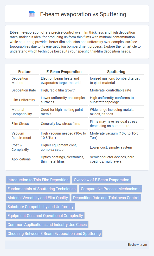
Table of Comparison
| Feature | E-Beam Evaporation | Sputtering |
|---|---|---|
| Deposition Method | Electron beam heats and evaporates target material | Ionized gas ions bombard target to eject material |
| Deposition Rate | High, rapid film growth | Moderate, controllable rate |
| Film Uniformity | Lower uniformity on complex surfaces | High uniformity, conforms to substrate topology |
| Material Compatibility | Good for high melting point metals | Wide range including metals, oxides, nitrides |
| Film Stress | Generally low stress films | Films may have residual stress depending on parameters |
| Vacuum Requirement | High vacuum needed (10-6 to 10-8 Torr) | Moderate vacuum (10-3 to 10-5 Torr) |
| Cost & Complexity | Higher equipment cost, complex setup | Lower cost, simpler system |
| Applications | Optics coatings, electronics, thin metal films | Semiconductor devices, hard coatings, multilayers |
Introduction to Thin Film Deposition
Thin film deposition techniques like e-beam evaporation and sputtering are essential for creating uniform coatings in semiconductor and optical industries. E-beam evaporation uses a focused electron beam to heat and vaporize target material, producing high-purity films with a directional flux, while sputtering employs ionized gas to eject atoms from a target, allowing better step coverage and film adhesion. Your choice depends on application-specific requirements such as film density, deposition rate, and substrate sensitivity.
Overview of E-Beam Evaporation
E-Beam evaporation utilizes a high-energy electron beam to heat and vaporize target materials within a vacuum, enabling precise thin-film deposition. This method offers superior control over film thickness and composition, making it ideal for applications requiring uniform coatings such as optics and electronics. Your choice of e-beam evaporation can significantly enhance film purity and deposition rate compared to sputtering techniques.
Fundamentals of Sputtering Techniques
Sputtering techniques rely on the kinetic energy transfer from energetic ions to a target material, causing atoms to be ejected and deposited onto a substrate, enabling precise thin film formation. Unlike e-beam evaporation, which uses thermal energy to vaporize materials, sputtering offers superior control over film composition, uniformity, and adhesion due to its physical bombardment process. Your choice between these methods affects factors like deposition rate, film density, and the ability to coat complex geometries effectively.
Comparative Process Mechanisms
E-beam evaporation uses a focused electron beam to vaporize material from a target, producing a high-purity thin film with directional deposition but limited step coverage. In contrast, sputtering relies on ion bombardment of the target, ejecting atoms with more uniform angular distribution, resulting in better step coverage and adhesion. Your choice between e-beam evaporation and sputtering depends on the desired film uniformity, material compatibility, and substrate geometry.
Material Versatility and Film Quality
E-beam evaporation offers high material versatility by efficiently depositing metals, oxides, and complex compounds with precise control over the evaporation rate, resulting in smooth, dense films ideal for microelectronics and optics. Sputtering provides superior film quality with excellent adhesion and uniformity across complex substrates, making it suitable for thin films requiring high density and stoichiometric accuracy, especially for metals, alloys, and insulating materials. The choice depends on specific application requirements, with e-beam faster for deposition rates and sputtering better for conformal coating and film integrity.
Deposition Rate and Thickness Control
E-beam evaporation offers higher deposition rates, often exceeding several nanometers per second, which enables rapid thin-film growth but with less uniform thickness control over large substrates. Sputtering provides more precise thickness control through adjustable process parameters like power and pressure, resulting in uniform films even on complex substrate geometries. The choice between e-beam evaporation and sputtering depends on the required balance between deposition speed and nanoscale thickness uniformity for applications such as semiconductor device fabrication or optical coatings.
Substrate Compatibility and Uniformity
E-beam evaporation offers excellent compatibility with temperature-sensitive substrates due to its relatively low substrate heating during deposition, making it ideal for polymers and delicate materials. Sputtering provides superior film uniformity and step coverage, especially on complex topographies, thanks to its energetic plasma environment that promotes better adhesion and conformal coatings. Selecting between e-beam evaporation and sputtering depends on balancing substrate thermal tolerance with the need for uniform, dense films in applications like semiconductor fabrication and optical coatings.
Equipment Cost and Operational Complexity
E-beam evaporation generally involves lower initial equipment costs compared to sputtering systems, making it more accessible for smaller-scale operations. However, sputtering offers greater operational complexity with its need for precise plasma control and gas management, which can increase maintenance and training requirements. Your choice depends on balancing budget constraints against the desired film quality and process stability.
Common Applications and Industry Use Cases
E-beam evaporation is commonly used in the semiconductor industry for depositing high-purity thin films such as metals and dielectrics in microelectronics and optics manufacturing. Sputtering is widely applied in hard disk drive coatings, solar cells, and decorative finishes due to its ability to deposit uniform and adherent films on complex substrates. Both techniques are essential in producing thin films for flexible electronics, display technologies, and protective coatings in aerospace and automotive industries.
Choosing Between E-Beam Evaporation and Sputtering
Choosing between e-beam evaporation and sputtering depends on your coating requirements and material properties. E-beam evaporation offers high deposition rates and is ideal for materials with high melting points, while sputtering provides better film adhesion and uniformity, especially on complex surfaces. For applications demanding precise thickness control and dense films, sputtering often outperforms e-beam evaporation.
e-beam evaporation vs sputtering Infographic