Plasma etching offers precise, anisotropic material removal by using ionized gases, making it ideal for microfabrication and semiconductor processes, while wet etching relies on chemical solutions to isotropically dissolve materials, which can lead to undercutting but is simpler and less costly. Explore the rest of this article to understand which etching method best suits your specific application needs.
Table of Comparison
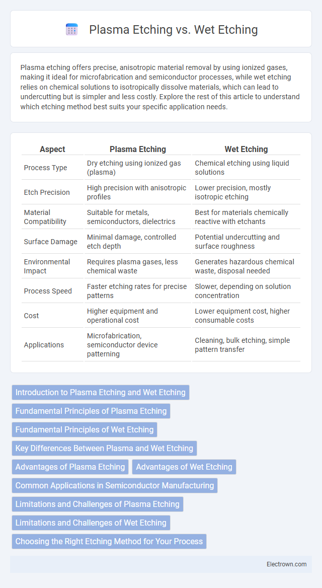
| Aspect | Plasma Etching | Wet Etching |
|---|---|---|
| Process Type | Dry etching using ionized gas (plasma) | Chemical etching using liquid solutions |
| Etch Precision | High precision with anisotropic profiles | Lower precision, mostly isotropic etching |
| Material Compatibility | Suitable for metals, semiconductors, dielectrics | Best for materials chemically reactive with etchants |
| Surface Damage | Minimal damage, controlled etch depth | Potential undercutting and surface roughness |
| Environmental Impact | Requires plasma gases, less chemical waste | Generates hazardous chemical waste, disposal needed |
| Process Speed | Faster etching rates for precise patterns | Slower, depending on solution concentration |
| Cost | Higher equipment and operational cost | Lower equipment cost, higher consumable costs |
| Applications | Microfabrication, semiconductor device patterning | Cleaning, bulk etching, simple pattern transfer |
Introduction to Plasma Etching and Wet Etching
Plasma etching uses ionized gases to remove material from a substrate with high precision, making it essential in semiconductor manufacturing for creating intricate microstructures. Wet etching employs liquid chemical solutions to selectively dissolve materials, offering simplicity and cost-effectiveness but less control over feature dimensions. Both techniques play critical roles in microfabrication, with plasma etching preferred for anisotropic patterns and wet etching suited for isotropic material removal.
Fundamental Principles of Plasma Etching
Plasma etching utilizes ionized gases to remove material through chemical reactions and physical sputtering, offering precise control over etch profiles and selectivity compared to wet etching, which relies on liquid chemical solutions for material removal. The plasma environment generates reactive species such as radicals and ions that interact with the substrate, enabling anisotropic etching crucial for semiconductor fabrication and microelectronics. This dry etching technique provides superior uniformity and reduced contamination, making it essential for advanced device manufacturing processes.
Fundamental Principles of Wet Etching
Wet etching relies on chemical solutions to selectively dissolve materials from a substrate, utilizing isotropic reactions that etch uniformly in all directions. This method involves immersion or spraying of the substrate with acids or bases, which react with specific layers to remove them based on their chemical composition. The process is widely used for its simplicity and cost-effectiveness in microfabrication, though it typically offers lower precision and less anisotropic control compared to plasma etching.
Key Differences Between Plasma and Wet Etching
Plasma etching utilizes ionized gases to selectively remove material through physical and chemical reactions, offering high precision and anisotropic profiles ideal for microfabrication. Wet etching employs liquid chemical solutions to dissolve target layers, providing simpler processing but typically resulting in isotropic etching with less control over feature dimensions. The choice between plasma and wet etching depends on factors like etch rate, selectivity, feature resolution, and substrate compatibility.
Advantages of Plasma Etching
Plasma etching offers precise control over the etching process, enabling high-resolution patterning crucial for semiconductor manufacturing and microfabrication. It provides superior anisotropy compared to wet etching, allowing vertical sidewalls and minimizing undercutting, which enhances device performance. The dry nature of plasma etching reduces chemical waste and contamination risks, supporting cleaner workflows and improved compatibility with complex, multi-layered materials.
Advantages of Wet Etching
Wet etching offers precise isotropic material removal, making it ideal for complex microfabrication tasks requiring uniform etching in multiple directions. The process is cost-effective and simpler, utilizing common chemicals like hydrofluoric acid, which reduces equipment expenses compared to the high-vacuum systems required for plasma etching. Wet etching's high etch rates enhance throughput and efficiency, particularly beneficial for large-scale semiconductor manufacturing and thin-film patterning.
Common Applications in Semiconductor Manufacturing
Plasma etching is commonly used for precise pattern transfer and fine feature definition in advanced semiconductor manufacturing, especially in the fabrication of integrated circuits and MEMS devices. Wet etching is typically applied for bulk material removal and surface cleaning due to its simplicity and cost-effectiveness, often in the production of silicon wafers and larger microstructures. Your choice between plasma and wet etching impacts process control, resolution, and overall device performance in semiconductor fabrication.
Limitations and Challenges of Plasma Etching
Plasma etching faces limitations such as surface damage and microloading effects, which can reduce etch uniformity and precision in semiconductor fabrication. The process struggles with high aspect ratio etching due to ion directionality constraints, limiting its effectiveness for complex nanostructures. Furthermore, plasma etching requires stringent control over gas chemistry and plasma parameters to avoid contamination and inconsistencies, increasing operational complexity and cost.
Limitations and Challenges of Wet Etching
Wet etching faces limitations such as isotropic material removal, which can cause undercutting and reduced pattern fidelity compared to plasma etching's anisotropic precision. Chemical selectivity in wet etching is often less controllable, leading to potential damage of adjacent layers and reduced process uniformity. Your fabrication processes may encounter challenges like difficulty in etching complex geometries and managing hazardous chemical waste disposal.
Choosing the Right Etching Method for Your Process
Selecting between plasma etching and wet etching depends on factors like material type, desired precision, and process environment. Plasma etching offers superior anisotropy and fine feature control, ideal for semiconductor fabrication, while wet etching provides faster removal rates for less intricate patterns and larger areas. Assess your process requirements, including etch uniformity and compatibility with masking materials, to determine the optimal method for your application.
plasma etching vs wet etching Infographic