E-beam lithography offers unparalleled precision for creating nanoscale patterns, surpassing photolithography's resolution limitations by directly writing designs with a focused electron beam, although it is generally slower and more costly. Explore the rest of this article to compare how each technique impacts Your semiconductor fabrication needs and determine which method best suits Your application.
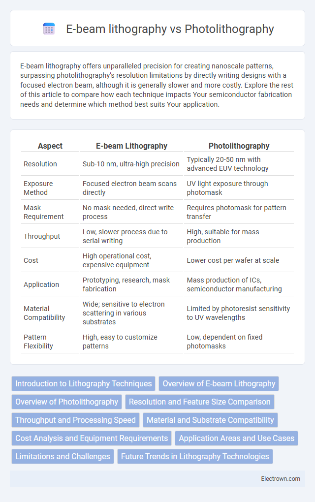
Table of Comparison
| Aspect | E-beam Lithography | Photolithography |
|---|---|---|
| Resolution | Sub-10 nm, ultra-high precision | Typically 20-50 nm with advanced EUV technology |
| Exposure Method | Focused electron beam scans directly | UV light exposure through photomask |
| Mask Requirement | No mask needed, direct write process | Requires photomask for pattern transfer |
| Throughput | Low, slower process due to serial writing | High, suitable for mass production |
| Cost | High operational cost, expensive equipment | Lower cost per wafer at scale |
| Application | Prototyping, research, mask fabrication | Mass production of ICs, semiconductor manufacturing |
| Material Compatibility | Wide; sensitive to electron scattering in various substrates | Limited by photoresist sensitivity to UV wavelengths |
| Pattern Flexibility | High, easy to customize patterns | Low, dependent on fixed photomasks |
Introduction to Lithography Techniques
E-beam lithography utilizes a focused electron beam to write custom patterns directly onto a resist-coated substrate, offering nanometer-scale precision for advanced semiconductor device fabrication. Photolithography employs ultraviolet light through a mask to transfer circuit patterns onto substrates, enabling high-throughput production but limited by diffraction limits to feature sizes around tens of nanometers. Your choice between these techniques depends on the required resolution, production volume, and cost constraints in semiconductor manufacturing.
Overview of E-beam Lithography
E-beam lithography uses a focused beam of electrons to create extremely precise patterns on a semiconductor substrate, enabling feature sizes below 10 nanometers essential for advanced microelectronics and nanotechnology applications. Unlike photolithography that relies on ultraviolet light and masks, E-beam offers maskless direct writing, allowing high resolution and flexibility in prototyping and low-volume production. Your choice of E-beam lithography supports intricate designs but requires longer processing times and higher costs compared to photolithography.
Overview of Photolithography
Photolithography is a widely used semiconductor manufacturing process that employs ultraviolet light to transfer geometric patterns from a photomask onto a photosensitive resist layer on a substrate. It offers high throughput and excellent resolution suitable for mass production of integrated circuits and microelectromechanical systems. Your choice of photolithography enables precise patterning for devices with features typically down to several nanometers, balancing cost-effectiveness and scalability.
Resolution and Feature Size Comparison
E-beam lithography achieves significantly higher resolution compared to photolithography, reaching feature sizes as small as 10 nanometers due to its ability to directly write patterns with a focused electron beam. Photolithography typically produces feature sizes limited to around 45 nanometers in advanced semiconductor manufacturing, constrained by the wavelength of ultraviolet light and mask technology. The superior resolution of e-beam lithography makes it ideal for prototyping and fabricating nanoscale devices where precise patterning is critical.
Throughput and Processing Speed
E-beam lithography offers superior resolution but significantly lower throughput and slower processing speed compared to photolithography, making it less suitable for mass production. Photolithography excels in high-throughput manufacturing environments with rapid processing capabilities, enabling efficient wafer-scale patterning. Your choice hinges on balancing the need for fine feature detail against production speed demands in semiconductor fabrication.
Material and Substrate Compatibility
E-beam lithography offers superior resolution and patterning precision on a wide range of materials including non-planar and sensitive substrates, making it ideal for research and prototype development on silicon, glass, and flexible polymers. Photolithography, optimized for high-throughput semiconductor manufacturing, primarily supports silicon wafers with photoresists sensitive to UV light but faces limitations with non-standard or non-flat substrates. The compatibility of e-beam lithography with diverse materials and complex substrate topographies provides a key advantage over photolithography in advanced nanofabrication applications.
Cost Analysis and Equipment Requirements
E-beam lithography requires highly specialized, expensive equipment with precise electron beam control, leading to significant upfront and maintenance costs compared to photolithography's more affordable, widely available optical systems. Photolithography benefits from faster processing speeds and lower per-unit costs, making it more cost-effective for high-volume semiconductor manufacturing. Your choice depends on balancing budget constraints with the need for superior resolution and patterning flexibility offered by E-beam lithography.
Application Areas and Use Cases
E-beam lithography is predominantly used in research and development for fabricating nanoscale features in quantum devices, photonic crystals, and semiconductor prototypes due to its high resolution and precision. Photolithography dominates mass production in the semiconductor industry for manufacturing integrated circuits, microelectromechanical systems (MEMS), and displays, thanks to its fast throughput and scalability for large wafers. Your choice between E-beam lithography and photolithography depends on whether you require nanometer-scale patterning for specialized applications or high-volume, cost-effective manufacturing for commercial electronics.
Limitations and Challenges
E-beam lithography faces limitations in throughput and scalability due to its serial writing process, making it less suitable for high-volume manufacturing compared to photolithography. Photolithography encounters challenges in achieving sub-10nm resolution because of light diffraction limits and the complexity of extreme ultraviolet (EUV) source generation. Both technologies struggle with resist sensitivity and pattern fidelity, impacting overall device performance and production cost.
Future Trends in Lithography Technologies
E-beam lithography offers unmatched resolution for nanoscale patterning, driving innovations in semiconductor manufacturing as device features shrink below 5 nm. Photolithography continues to evolve with extreme ultraviolet (EUV) technology, enhancing throughput and cost-efficiency for mass production of advanced integrated circuits. Your choice between these methods depends on balancing precision needs with volume requirements, as hybrid approaches may dominate future lithography trends in the semiconductor industry.
E-beam lithography vs Photolithography Infographic