InP (Indium Phosphide) and GaAs (Gallium Arsenide) are semiconductor materials widely used in high-frequency and optoelectronic applications, with InP offering superior electron mobility and efficiency at higher frequencies while GaAs provides cost-effective solutions with high electron velocity. Understanding the distinct advantages and limitations of these compounds will help you make informed decisions for your specific technology needs; explore the full article to dive deeper into their comparative performance and uses.
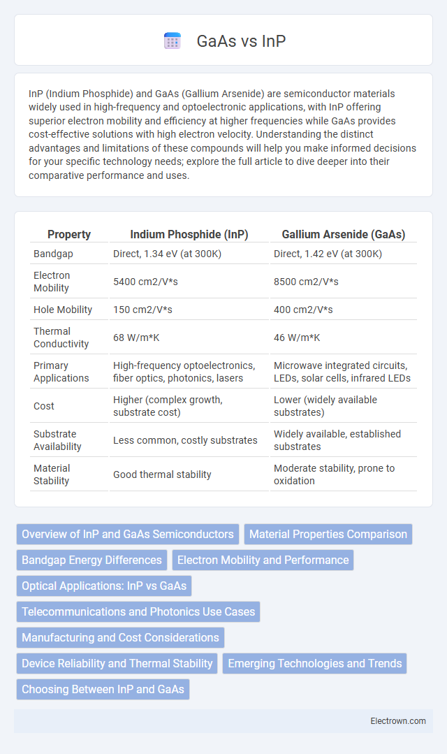
Table of Comparison
| Property | Indium Phosphide (InP) | Gallium Arsenide (GaAs) |
|---|---|---|
| Bandgap | Direct, 1.34 eV (at 300K) | Direct, 1.42 eV (at 300K) |
| Electron Mobility | 5400 cm2/V*s | 8500 cm2/V*s |
| Hole Mobility | 150 cm2/V*s | 400 cm2/V*s |
| Thermal Conductivity | 68 W/m*K | 46 W/m*K |
| Primary Applications | High-frequency optoelectronics, fiber optics, photonics, lasers | Microwave integrated circuits, LEDs, solar cells, infrared LEDs |
| Cost | Higher (complex growth, substrate cost) | Lower (widely available substrates) |
| Substrate Availability | Less common, costly substrates | Widely available, established substrates |
| Material Stability | Good thermal stability | Moderate stability, prone to oxidation |
Overview of InP and GaAs Semiconductors
Indium Phosphide (InP) is a III-V semiconductor known for its high electron velocity and superior performance in high-frequency and high-power applications, while Gallium Arsenide (GaAs) offers excellent electron mobility and intrinsic radiation resistance, making it ideal for optoelectronic devices and microwave frequency circuits. Both materials exhibit direct bandgaps, with InP having a bandgap of about 1.34 eV and GaAs about 1.42 eV, influencing their efficiency in light emission and absorption. Your choice between InP and GaAs depends on device requirements such as operating speed, wavelength, and environmental robustness.
Material Properties Comparison
InP (Indium Phosphide) offers higher electron mobility and better thermal conductivity compared to GaAs (Gallium Arsenide), making it ideal for high-frequency and high-power applications. GaAs provides a wider direct bandgap of about 1.42 eV compared to InP's 1.34 eV, enabling better performance in optoelectronic devices like LEDs and laser diodes. When selecting semiconductor materials, your choice between InP and GaAs will impact device speed, efficiency, and thermal management based on these intrinsic properties.
Bandgap Energy Differences
Indium Phosphide (InP) exhibits a direct bandgap energy of approximately 1.34 eV at room temperature, while Gallium Arsenide (GaAs) has a slightly higher direct bandgap energy of about 1.42 eV. This difference in bandgap energies affects their optical absorption and emission properties, making GaAs more efficient for applications involving shorter wavelengths such as visible light. In contrast, InP is preferred for devices operating in the near-infrared region, particularly in fiber-optic communication systems.
Electron Mobility and Performance
Indium Phosphide (InP) exhibits significantly higher electron mobility than Gallium Arsenide (GaAs), with values around 12,000 cm2/V*s compared to GaAs's 8,500 cm2/V*s, enabling faster electron transport and improved device speed. This superior electron mobility directly translates to enhanced high-frequency performance in InP-based transistors and integrated circuits, making InP the preferred choice for ultra-high-speed photonics and microwave applications. Consequently, InP devices demonstrate lower noise figures and higher cutoff frequencies, outperforming GaAs in applications demanding exceptional frequency response and signal integrity.
Optical Applications: InP vs GaAs
Indium Phosphide (InP) offers superior performance in high-speed optical communication systems due to its direct bandgap and higher electron mobility, enabling efficient laser diodes and photodetectors operating at wavelengths around 1.3 to 1.55 microns, critical for fiber-optic networks. Gallium Arsenide (GaAs) is preferred for optoelectronic devices at shorter wavelengths near 0.85 microns, such as LEDs and photodetectors in optical storage or sensing applications, due to its mature fabrication technology and material properties. Your choice between InP and GaAs for optical applications will depend on the required wavelength range and device speed, with InP dominating telecom wavelengths and GaAs serving visible to near-infrared uses.
Telecommunications and Photonics Use Cases
In telecommunications and photonics, InP (Indium Phosphide) outperforms GaAs (Gallium Arsenide) in high-speed optical communication systems due to its superior electron mobility and direct bandgap, enabling efficient laser diodes and photodetectors operating at 1.3 to 1.55 um wavelengths. GaAs remains valuable for lower-frequency microwave photonics and optoelectronic applications given its mature fabrication technology and cost advantages. Your choice between InP and GaAs hinges on the required wavelength compatibility, device speed, and integration complexity for cutting-edge telecommunication infrastructure.
Manufacturing and Cost Considerations
InP (Indium Phosphide) substrates typically incur higher manufacturing costs than GaAs (Gallium Arsenide) due to more complex crystal growth and wafer fabrication processes. GaAs benefits from well-established, cost-effective manufacturing infrastructure and larger wafer sizes, enabling economies of scale. The cost disparity influences material selection, with GaAs favored for budget-sensitive, high-volume applications, while InP is chosen for high-performance devices despite its premium price.
Device Reliability and Thermal Stability
InP devices exhibit superior thermal stability due to their wider bandgap and higher electron mobility, making them more resilient under high-temperature conditions compared to GaAs. GaAs devices can suffer from increased leakage currents and degraded performance at elevated temperatures, impacting long-term device reliability. If your application demands robust operation in harsh thermal environments, choosing InP technology ensures enhanced device reliability and sustained performance.
Emerging Technologies and Trends
Indium Phosphide (InP) dominates emerging high-speed photonics and quantum computing applications due to its superior electron mobility and direct bandgap properties, enabling faster data transmission and efficient laser integration. Gallium Arsenide (GaAs) remains a key material in millimeter-wave applications and power amplifiers for 5G technology, benefiting from its mature fabrication processes and high electron velocity. Recent trends highlight InP's increasing role in integrated photonic circuits (PICs) for optical communication, while GaAs adapts to evolving RF front-end modules in next-generation wireless networks.
Choosing Between InP and GaAs
Choosing between Indium Phosphide (InP) and Gallium Arsenide (GaAs) depends on specific application requirements such as frequency range, electron mobility, and device efficiency. InP offers superior electron velocity and higher frequency performance ideal for high-speed optoelectronics and fiber-optic communication systems, while GaAs provides cost-effective manufacturing with good electron mobility suited for microwave and RF applications. The decision hinges on trade-offs between performance demands and material cost, with InP preferred for ultra-high-frequency devices and GaAs for widely deployed, cost-sensitive technologies.
InP vs GaAs Infographic