MEMS and NEMS differ primarily in scale, with MEMS (Micro-Electro-Mechanical Systems) operating at the micrometer level and NEMS (Nano-Electro-Mechanical Systems) functioning at the nanometer scale, enabling more sensitive and precise applications. Explore the rest of the article to understand how these technologies impact your device performance and innovation potential.
Table of Comparison
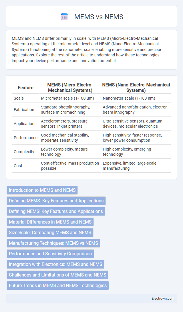
| Feature | MEMS (Micro-Electro-Mechanical Systems) | NEMS (Nano-Electro-Mechanical Systems) |
|---|---|---|
| Scale | Micrometer scale (1-100 um) | Nanometer scale (1-100 nm) |
| Fabrication | Standard photolithography, surface micromachining | Advanced nanofabrication, electron beam lithography |
| Applications | Accelerometers, pressure sensors, inkjet printers | Ultra-sensitive sensors, quantum devices, molecular electronics |
| Performance | Good mechanical stability, moderate sensitivity | High sensitivity, faster response, lower power consumption |
| Complexity | Lower complexity, mature technology | High complexity, emerging technology |
| Cost | Cost-effective, mass production possible | Expensive, limited large-scale manufacturing |
Introduction to MEMS and NEMS
MEMS (Micro-Electro-Mechanical Systems) and NEMS (Nano-Electro-Mechanical Systems) represent advancements in miniaturized technology, with MEMS operating at the micrometer scale and NEMS at the nanometer scale. MEMS integrate mechanical elements, sensors, actuators, and electronics on a common silicon substrate, widely used in automotive sensors and inkjet printer heads. NEMS push this integration further by enabling improved sensitivity, faster response, and lower power consumption in applications such as quantum computing and highly sensitive biological sensors.
Defining MEMS: Key Features and Applications
MEMS (Micro-Electro-Mechanical Systems) are microscale devices integrating mechanical elements, sensors, actuators, and electronics on a silicon substrate, enabling precise control and sensing at the micrometer scale. Key features of MEMS include miniaturization, low power consumption, high reliability, and batch fabrication compatibility, making them essential in automotive sensors, medical devices, and consumer electronics. Applications span from accelerometers in smartphones and airbag sensors in vehicles to lab-on-chip systems and inkjet printer heads, highlighting their versatility and impact in various industries.
Defining NEMS: Key Features and Applications
NEMS (Nanoelectromechanical Systems) operate at the nanoscale, enabling ultra-sensitive sensing and ultra-fast signal processing beyond MEMS capabilities. Key features include exceptional mechanical resonance frequencies, reduced power consumption, and atomic-scale precision in components. Your innovations can leverage NEMS for cutting-edge applications in quantum computing, biochemical sensing, and advanced nanorobotics.
Material Differences in MEMS and NEMS
MEMS (Micro-Electro-Mechanical Systems) primarily use silicon-based materials like single-crystal silicon and polysilicon due to their mechanical robustness and established fabrication processes. NEMS (Nano-Electro-Mechanical Systems) incorporate advanced materials including graphene, carbon nanotubes, and other two-dimensional materials to achieve superior electrical, mechanical, and thermal properties at the nanoscale. The material selection in NEMS emphasizes atomic-scale precision and quantum effects, enabling enhanced sensitivity and energy efficiency compared to traditional MEMS devices.
Size Scale: Comparing MEMS and NEMS
MEMS (Micro-Electromechanical Systems) operate at the micrometer scale, typically ranging from 1 to 100 micrometers, while NEMS (Nano-Electromechanical Systems) function at the nanometer scale, often below 100 nanometers. This size difference significantly impacts sensitivity, power consumption, and integration density, with NEMS offering enhanced performance due to their smaller dimensions. Your choice between MEMS and NEMS depends on the application's precision requirements and space constraints.
Manufacturing Techniques: MEMS vs NEMS
MEMS manufacturing primarily employs photolithography, bulk micromachining, and surface micromachining techniques to create microscale structures on silicon substrates. NEMS fabrication involves more advanced processes like electron beam lithography, atomic layer deposition, and focused ion beam milling to achieve nanoscale precision and smaller feature sizes. Your choice between MEMS and NEMS manufacturing techniques depends on the required resolution, complexity, and application scale.
Performance and Sensitivity Comparison
MEMS (Micro-Electro-Mechanical Systems) and NEMS (Nano-Electro-Mechanical Systems) exhibit distinct performance and sensitivity characteristics due to their size differences. NEMS devices provide significantly higher sensitivity and faster response times than MEMS, attributed to their nanoscale dimensions, which enhance signal detection at atomic or molecular levels. Your choice between MEMS and NEMS should consider the specific application requirements for precision, with NEMS being ideal for ultra-sensitive detection and MEMS suitable for robust, larger-scale sensing tasks.
Integration with Electronics: MEMS and NEMS
MEMS (Micro-Electro-Mechanical Systems) offer seamless integration with standard semiconductor electronics, enabling efficient signal processing and compact device architecture. NEMS (Nano-Electro-Mechanical Systems) leverage their nanoscale dimensions to achieve ultra-high sensitivity and faster response times, but their integration with conventional electronics presents greater fabrication complexity. Understanding the integration challenges between MEMS and NEMS helps you select the optimal technology for advanced electronic and sensing applications.
Challenges and Limitations of MEMS and NEMS
MEMS (Micro-Electro-Mechanical Systems) face challenges including limited sensitivity, fabrication complexity, and integration issues with electronic components. NEMS (Nano-Electro-Mechanical Systems) encounter limitations such as higher surface-to-volume ratios causing increased stiction, reduced device reliability, and difficulties in mass production due to nanoscale precision requirements. Both MEMS and NEMS must overcome material constraints, scalability barriers, and thermal management problems to achieve widespread commercial applications.
Future Trends in MEMS and NEMS Technologies
Future trends in MEMS and NEMS technologies emphasize enhanced sensitivity, miniaturization, and integration with AI for smart systems. NEMS devices are projected to dominate ultra-sensitive applications in healthcare and environmental monitoring due to their atomic-scale precision. Your next-generation innovations will benefit from combining MEMS scalability with NEMS' quantum-level performance for advanced IoT and wearable devices.
MEMS vs NEMS Infographic