Leadless packages offer improved thermal performance and reduced electrical parasitics compared to traditional leaded packages, making them ideal for compact, high-frequency applications. Explore the rest of the article to understand which package suits your specific electronic design needs.
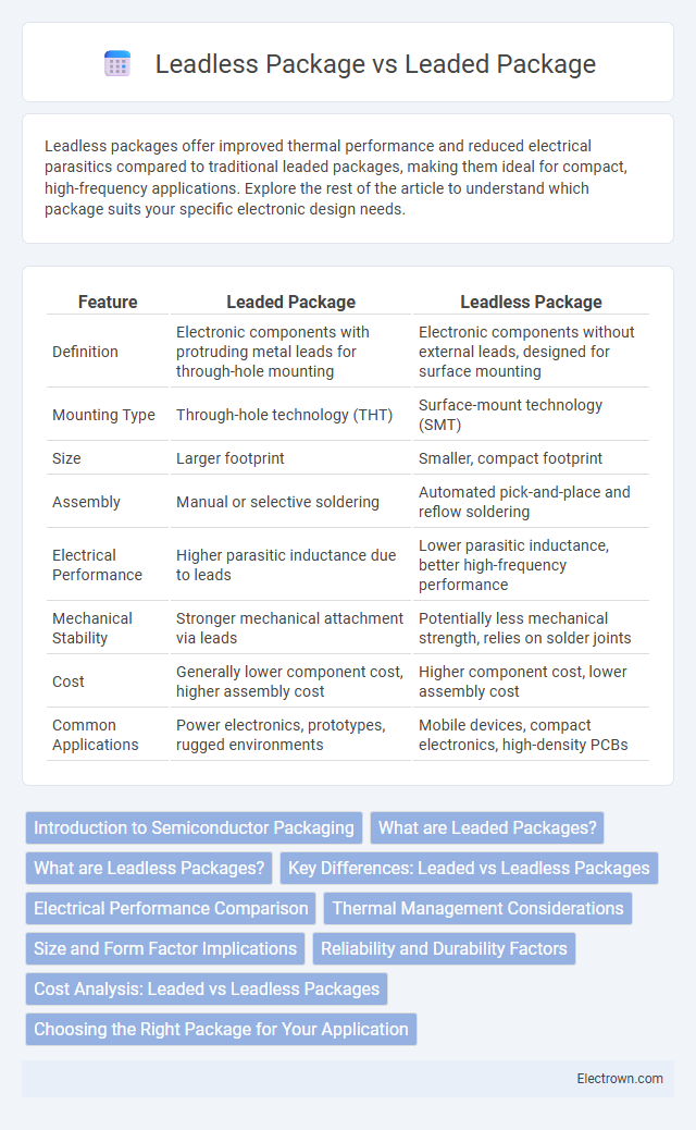
Table of Comparison
| Feature | Leaded Package | Leadless Package |
|---|---|---|
| Definition | Electronic components with protruding metal leads for through-hole mounting | Electronic components without external leads, designed for surface mounting |
| Mounting Type | Through-hole technology (THT) | Surface-mount technology (SMT) |
| Size | Larger footprint | Smaller, compact footprint |
| Assembly | Manual or selective soldering | Automated pick-and-place and reflow soldering |
| Electrical Performance | Higher parasitic inductance due to leads | Lower parasitic inductance, better high-frequency performance |
| Mechanical Stability | Stronger mechanical attachment via leads | Potentially less mechanical strength, relies on solder joints |
| Cost | Generally lower component cost, higher assembly cost | Higher component cost, lower assembly cost |
| Common Applications | Power electronics, prototypes, rugged environments | Mobile devices, compact electronics, high-density PCBs |
Introduction to Semiconductor Packaging
Semiconductor packaging protects the integrated circuit and facilitates electrical connections to the PCB, with leaded packages featuring external metal leads for soldering and leadless packages offering compact, lead-free soldering pads. Leaded packages like Dual In-line Package (DIP) simplify hand soldering and prototyping, while leadless designs such as QFN (Quad Flat No-lead) enable better thermal performance and higher pin density in compact devices. Your choice between leaded and leadless packaging impacts assembly methods, device longevity, and overall electronic system reliability.
What are Leaded Packages?
Leaded packages are electronic component enclosures featuring metal leads or pins that extend from the package body, allowing for through-hole mounting on printed circuit boards (PCBs). These leads provide mechanical support and electrical connections, commonly found in DIP (Dual Inline Package) and TO-220 types. Their design facilitates easier manual soldering and inspection compared to leadless packages.
What are Leadless Packages?
Leadless packages are electronic component housings designed without external leads, improving performance by reducing parasitic inductance and capacitance. These packages often use flat contacts or pads on the underside, enabling better heat dissipation and enabling higher-density circuit board layouts. Your choice of leadless packages can enhance product reliability and miniaturization in modern electronic designs.
Key Differences: Leaded vs Leadless Packages
Leaded packages feature external metal leads for easy soldering and mechanical stability, whereas leadless packages rely on metal pads or contacts beneath the component, enabling a compact design and improved electrical performance. Leaded types generally offer better heat dissipation and ease of prototyping, while leadless packages excel in automated assembly and space-saving applications. Understanding these key differences helps optimize Your PCB layout and manufacturing process choices.
Electrical Performance Comparison
Leaded packages typically offer superior electrical performance due to lower parasitic inductance and capacitance, which enhances signal integrity and reduces electromagnetic interference (EMI) in high-frequency applications. Leadless packages, such as QFN or DFN, provide shorter electrical paths that minimize resistance and inductance, improving thermal performance and enabling higher data rates in compact designs. The choice between leaded and leadless packages depends on specific requirements for impedance control, signal speed, and board space efficiency in electronic circuits.
Thermal Management Considerations
Leaded packages typically offer superior thermal dissipation due to their exposed leads and larger surface area, which facilitate efficient heat transfer away from the semiconductor die. Leadless packages, such as QFN or DFN, rely on an exposed pad beneath the device for thermal conduction, requiring careful PCB design with thermal vias and copper pours to optimize heat dissipation. Effective thermal management in leadless packages depends heavily on board layout and solder joint integrity to prevent overheating and ensure device reliability.
Size and Form Factor Implications
Leadless packages have a smaller footprint and lower profile compared to traditional leaded packages, making them ideal for compact electronic designs and high-density circuit boards. The absence of protruding leads reduces parasitic inductance and capacitance, enhancing signal integrity and thermal performance in tightly packed assemblies. Leaded packages, while bulkier, offer easier hand-soldering and mechanical robustness, often preferred in prototyping and applications with less stringent size constraints.
Reliability and Durability Factors
Leaded packages generally offer robust mechanical stability due to their soldered leads, making them more resistant to physical stress and thermal cycling. Leadless packages, like QFNs or DFNs, minimize inductance and improve thermal performance but may be more susceptible to solder joint cracking under extreme mechanical strain. Understanding these reliability and durability factors helps you select the best package for long-term electronic device performance.
Cost Analysis: Leaded vs Leadless Packages
Leaded packages generally incur higher manufacturing and assembly costs due to their larger size and additional materials like metal leads. Leadless packages, such as chip-scale packages (CSP), reduce costs by minimizing material usage and enabling automated, high-density PCB assembly, which decreases labor and handling expenses. Your choice between leaded and leadless packages significantly impacts the overall cost efficiency of your electronics production.
Choosing the Right Package for Your Application
Selecting between leaded and leadless packages depends on your application's thermal and mechanical requirements. Leaded packages offer easier handling and soldering for prototyping or repair, while leadless packages provide better thermal performance and reduced parasitic inductance, ideal for high-frequency or space-constrained designs. Evaluating your product's assembly process, size limitations, and electrical performance will help determine the optimal package choice.
leaded vs leadless package Infographic