Edge plating enhances circuit board durability by applying a conductive layer around the board's perimeter, improving electromagnetic interference shielding and mechanical strength. Understanding these differences can help you choose the optimal plating method for your project; explore the article to learn more about edge plating vs via plating.
Table of Comparison
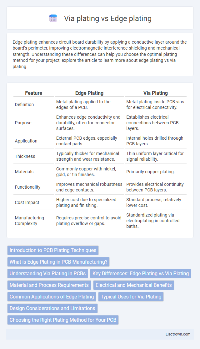
| Feature | Edge Plating | Via Plating |
|---|---|---|
| Definition | Metal plating applied to the edges of a PCB. | Metal plating inside PCB vias for electrical connectivity. |
| Purpose | Enhances edge conductivity and durability, often for connector surfaces. | Establishes electrical connections between PCB layers. |
| Application | External PCB edges, especially contact pads. | Internal holes drilled through PCB layers. |
| Thickness | Typically thicker for mechanical strength and wear resistance. | Thin uniform layer critical for signal reliability. |
| Materials | Commonly copper with nickel, gold, or tin finishes. | Primarily copper plating. |
| Functionality | Improves mechanical robustness and edge contacts. | Provides electrical continuity between PCB layers. |
| Cost Impact | Higher cost due to specialized plating and finishing. | Standard process, relatively lower cost. |
| Manufacturing Complexity | Requires precise control to avoid plating overflow or gaps. | Standardized plating via electroplating in controlled baths. |
Introduction to PCB Plating Techniques
PCB plating techniques such as edge plating and via plating serve critical roles in enhancing electrical connectivity and structural integrity. Edge plating creates continuous conductive pathways along the PCB's edges, improving grounding and EMI shielding, while via plating fills or coats drilled holes to establish reliable interlayer electrical connections. Understanding these methods helps optimize your PCB's performance and durability in complex electronic designs.
What is Edge Plating in PCB Manufacturing?
Edge plating in PCB manufacturing involves applying a conductive metal layer along the exposed edges of the printed circuit board, enhancing electrical connectivity and mechanical strength. This technique improves grounding and electromagnetic interference (EMI) shielding by creating a continuous conductive barrier around the PCB perimeter. Unlike via plating, which deposits metal inside drilled holes to connect different layers, edge plating specifically targets the PCB's outer edges for protection and performance optimization.
Understanding Via Plating in PCBs
Via plating in PCBs involves electroplating copper to create conductive pathways through drilled holes, enabling electrical connectivity between different layers. This process ensures signal integrity and mechanical strength, preventing faults in multilayer board designs. Understanding via plating helps you optimize PCB reliability and performance by improving interlayer connections compared to edge plating, which only coats the board's perimeter.
Key Differences: Edge Plating vs Via Plating
Edge plating involves plating the exposed edges of a printed circuit board (PCB) to provide enhanced mechanical strength and improved electrical connectivity across the board's perimeter. Via plating, on the other hand, refers to the process of electroplating the walls of via holes to establish reliable electrical connections between different layers within multi-layer PCBs. Key differences include edge plating targeting the PCB's outer boundaries for structural integrity and signal shielding, while via plating focuses on internal vertical interconnects critical for multilayer circuit functionality.
Material and Process Requirements
Edge plating requires specialized conductive materials like copper or nickel, applied through electroplating to ensure uniform coverage on PCB edges for enhanced shielding and durability. Via plating involves depositing copper within drilled holes using electroless copper deposition followed by electroplating to create reliable electrical connections between PCB layers. Both processes demand precise control over plating thickness and adhesion to maintain signal integrity and mechanical strength in high-performance electronics.
Electrical and Mechanical Benefits
Edge plating enhances electrical performance by providing a continuous conductive path along PCB edges, reducing signal impedance and electromagnetic interference. Via plating ensures reliable electrical connections between PCB layers, improving signal integrity and current carrying capacity. Your choice impacts mechanical strength as edge plating reinforces board edges against physical stress, while via plating increases structural stability within multilayer boards.
Common Applications of Edge Plating
Edge plating is commonly utilized in high-frequency and high-reliability printed circuit boards (PCBs) where electromagnetic interference (EMI) shielding and improved mechanical strength are critical. This technique is prevalent in aerospace, military, and medical device PCBs, enhancing signal integrity and structural durability. In contrast, via plating primarily serves to establish electrical connections between PCB layers, with common applications in multi-layer PCB designs for consumer electronics and telecommunications.
Typical Uses for Via Plating
Via plating is typically used to establish reliable electrical connections between multiple layers in printed circuit boards (PCBs), enabling signal transmission and power distribution throughout the board. It is essential in multilayer PCBs for through-hole vias, blind vias, and buried vias, providing robust conductivity and mechanical strength. Your PCB designs rely on via plating to maintain signal integrity and ensure manufacturing durability in high-density interconnects.
Design Considerations and Limitations
Edge plating requires precise board layout adjustments to ensure uniform copper thickness and electrical connectivity along the PCB's perimeter, with challenges in maintaining consistent plating on complex edges or cutouts. Via plating focuses on through-hole copper deposition, demanding careful control of aspect ratios and plating uniformity to prevent voids or weak interconnects, particularly for high-density or multilayer boards. Both techniques must address limitations in plating thickness, adhesion, and tolerance to thermal stress during manufacturing and operation.
Choosing the Right Plating Method for Your PCB
Choosing the right plating method for your PCB depends on the application requirements and design constraints. Edge plating offers enhanced electrical connectivity and improved EMI shielding by plating the PCB edges, ideal for high-frequency or high-current circuits. Via plating ensures reliable through-hole electrical connections and structural integrity by filling or plating vias, making it essential for multi-layer PCBs with complex routing needs.
Edge plating vs Via plating Infographic