PAD and VIA are essential elements in PCB design; a PAD serves as the area for component soldering, while a VIA facilitates electrical connections between different layers of the board. Understanding the differences and proper applications of each can enhance your PCB's performance and reliability--explore the rest of the article to learn more.
Table of Comparison
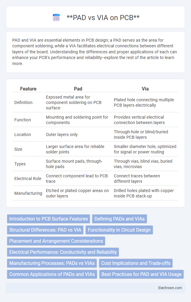
| Feature | Pad | Via |
|---|---|---|
| Definition | Exposed metal area for component soldering on PCB surface | Plated hole connecting multiple PCB layers electrically |
| Function | Mounting and soldering point for components | Provides vertical electrical connection between layers |
| Location | Outer layers only | Through-hole or blind/buried inside PCB layers |
| Size | Larger surface area for reliable solder joints | Smaller diameter hole, optimized for signal or power routing |
| Types | Surface mount pads, through-hole pads | Through vias, blind vias, buried vias, microvias |
| Electrical Role | Connect component lead to PCB trace | Connect traces between different layers |
| Manufacturing | Etched or plated copper areas on outer layers | Drilled holes plated with copper inside PCB stack-up |
Introduction to PCB Surface Features
PCB surface features, including pads and vias, play crucial roles in electronic circuit design and manufacturing. Pads serve as attachment points for components, ensuring stable mechanical and electrical connections, while vias provide conductive pathways between different layers of a multi-layer PCB. Understanding the distinct functions and locations of pads and vias is essential for optimizing circuit performance and fabrication efficiency.
Defining PADs and VIAs
PADs on a PCB are the exposed conductive areas where components are soldered; they provide electrical connections and mechanical support. VIAs are plated through holes that electrically connect different layers of the PCB, allowing signals and power to pass between layers. Your PCB design relies on precise placement and sizing of PADs and VIAs to ensure signal integrity and reliable component mounting.
Structural Differences: PAD vs VIA
Pads on PCBs are exposed conductive areas designed for component soldering, typically flat and positioned on the surface layer, whereas vias are plated through-holes that electrically connect different PCB layers by passing through the substrate. Pads have defined shapes and sizes to accommodate component leads or surface-mount device terminals, while vias are cylindrical structures with a metalized barrel ensuring vertical conductivity. The structural distinction lies in pads being surface features facilitating external connections, while vias serve as internal interlayer conduits essential for multilayer circuit routing.
Functionality in Circuit Design
PADs on PCBs serve as the designated points for component placement and soldering, ensuring reliable electrical connections and mechanical support for surface-mount or through-hole parts. VIAs facilitate electrical connectivity between different layers within a multi-layer PCB, enabling signal routing and power distribution without occupying surface space. Understanding the role of PADs and VIAs in your circuit design ensures optimal functionality by balancing component interfacing with efficient interlayer communication.
Placement and Arrangement Considerations
PADs on PCBs serve as the physical locations where components are soldered, requiring precise placement to ensure reliable electrical connections and mechanical stability. VIA placement must be strategically planned to optimize signal routing and minimize interference while maintaining PCB integrity, often positioned away from component pads to prevent solder bridging or shorts. Proper arrangement balances thermal management, signal integrity, and manufacturability, enhancing overall PCB performance and longevity.
Electrical Performance: Conductivity and Reliability
Pad design on PCBs directly impacts electrical performance by ensuring optimal conductivity through robust copper plating and precise surface finishes, which reduce resistance and signal loss. Via structures enhance reliability by providing consistent electrical connections between multiple PCB layers, with factors like via size, plating thickness, and aspect ratio playing critical roles in minimizing impedance and preventing failure under thermal and mechanical stress. The combined optimization of pads and vias is essential for maintaining signal integrity and long-term durability in high-frequency and high-current applications.
Manufacturing Processes: PADs vs VIAs
PADs serve as the primary surface points for component mounting and soldering on PCBs, fabricated through precise etching and plating processes to ensure reliable electrical connections. VIAs are small, plated-through holes that create vertical electrical pathways between different PCB layers, formed by drilling and electroplating techniques to maintain signal integrity and mechanical strength. Your PCB's performance depends on optimizing these manufacturing processes to balance conductivity, durability, and cost-efficiency.
Cost Implications and Trade-offs
Choosing between PAD and VIA on a PCB significantly affects cost implications and design trade-offs. PADs, used for component mounting, generally increase manufacturing complexity and material costs due to larger surface areas and plating requirements, whereas VIAs, essential for inter-layer connections, can reduce overall board size but may add drilling and plating expenses. Your decision should balance these factors based on the PCB's complexity and budget constraints to optimize both functionality and cost-efficiency.
Common Applications of PADs and VIAs
PADs on PCBs serve as connection points for surface-mounted components, facilitating soldering and electrical contact in devices like smartphones and computers. VIAs function as vertical interconnects, allowing signals and power to pass between multiple layers in multilayer PCBs, crucial for complex electronics such as aerospace systems and medical devices. Both PADs and VIAs are essential for ensuring reliable electrical connectivity and mechanical stability in densely packed circuit boards.
Best Practices for PAD and VIA Usage
Optimizing PAD and VIA usage on a PCB requires balancing electrical performance and manufacturability by selecting appropriate sizes and plating techniques to ensure reliable connections. You should place PADs with sufficient annular rings to prevent breakout and use VIAs with controlled drill-to-pad clearance to minimize signal integrity issues and enhance thermal management. Strategic distribution of VIAs aids in reducing inductance and resistance while maintaining mechanical strength across multilayer boards.
PAD vs VIA on PCB Infographic