GaN HEMTs offer higher power density and efficiency compared to GaAs FETs, making them ideal for high-frequency and high-power applications. Discover how these differences impact your electronic designs by reading the rest of the article.
Table of Comparison
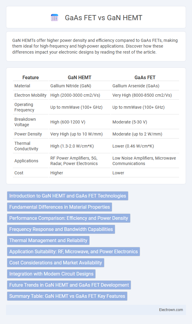
| Feature | GaN HEMT | GaAs FET |
|---|---|---|
| Material | Gallium Nitride (GaN) | Gallium Arsenide (GaAs) |
| Electron Mobility | High (2000-3000 cm2/Vs) | Very High (8000-8500 cm2/Vs) |
| Operating Frequency | Up to mmWave (100+ GHz) | Up to mmWave (100+ GHz) |
| Breakdown Voltage | High (600-1200 V) | Moderate (5-30 V) |
| Power Density | Very High (up to 10 W/mm) | Moderate (up to 2 W/mm) |
| Thermal Conductivity | High (1.3-2.0 W/cm*K) | Lower (0.46 W/cm*K) |
| Applications | RF Power Amplifiers, 5G, Radar, Power Electronics | Low Noise Amplifiers, Microwave Communications |
| Cost | Higher | Lower |
Introduction to GaN HEMT and GaAs FET Technologies
GaN HEMT (Gallium Nitride High Electron Mobility Transistor) technology offers superior electron mobility and higher breakdown voltage, enabling devices to operate efficiently at higher frequencies and power densities compared to GaAs FET (Gallium Arsenide Field Effect Transistor) technology. GaAs FETs, known for their mature fabrication processes and excellent noise performance, are widely used in low-noise amplifiers and microwave applications. The key distinction lies in GaN HEMT's wide bandgap material, which provides enhanced thermal conductivity and power handling, making it ideal for high-power RF and power electronics applications.
Fundamental Differences in Material Properties
GaN HEMTs utilize gallium nitride, a wide bandgap semiconductor with a bandgap energy of approximately 3.4 eV, enabling high breakdown voltage and superior thermal conductivity compared to GaAs FETs, which are based on gallium arsenide with a narrower bandgap of about 1.42 eV. These fundamental differences result in GaN HEMTs offering higher electron mobility and saturation velocity, making them ideal for high-power, high-frequency applications. GaAs FETs typically exhibit lower power density and thermal efficiency, limiting their performance in harsh or high-temperature environments.
Performance Comparison: Efficiency and Power Density
GaN HEMTs offer superior efficiency and higher power density compared to GaAs FETs, making them ideal for high-frequency and high-power applications. GaN devices can operate at higher voltages and temperatures, translating to better thermal management and reduced energy losses in your systems. This performance advantage enables more compact and efficient power amplifiers in telecommunications and radar technologies.
Frequency Response and Bandwidth Capabilities
GaN HEMT devices outperform GaAs FETs in frequency response and bandwidth capabilities due to their higher electron mobility and saturation velocity, enabling operation at frequencies exceeding 100 GHz. The superior material properties of GaN allow your circuits to achieve wider bandwidth and faster switching speeds essential for high-frequency applications like 5G and radar systems. GaAs FETs, while efficient at microwave frequencies, typically exhibit lower maximum frequency limits and narrower bandwidth compared to GaN HEMTs.
Thermal Management and Reliability
GaN HEMTs exhibit superior thermal conductivity compared to GaAs FETs, enabling efficient heat dissipation and maintaining performance under high power densities. Their robust material properties contribute to enhanced reliability in demanding applications, reducing the risk of thermal-induced failure. Your choice of GaN HEMT ensures better thermal management and longer device lifespan in high-frequency and high-power environments.
Application Suitability: RF, Microwave, and Power Electronics
GaN HEMTs excel in high-power RF and microwave applications due to their superior electron mobility, high breakdown voltage, and thermal stability, making them ideal for power amplifiers and radar systems. GaAs FETs offer lower noise figures and higher linearity, which suit low-noise amplifiers in communication and satellite systems operating at microwave frequencies. In power electronics, GaN HEMTs dominate because of their efficiency and fast switching capabilities, whereas GaAs FETs are less common due to their lower power handling and thermal limitations.
Cost Considerations and Market Availability
GaN HEMT devices generally offer higher power efficiency but come at a higher cost compared to GaAs FETs, which remain more affordable due to mature manufacturing processes and widespread market availability. GaAs FETs dominate lower-frequency applications given their cost-effectiveness and established supply chain, while GaN HEMTs are increasingly accessible for high-frequency, high-power markets despite limited vendor options. Your choice depends on balancing budget constraints with performance needs, as GaN technology is expanding but still experiences premium pricing relative to GaAs solutions.
Integration with Modern Circuit Designs
GaN HEMTs offer superior integration with modern circuit designs due to their higher electron mobility and power density, which enable more efficient high-frequency and high-power applications compared to GaAs FETs. The wide bandgap of GaN allows for better thermal management and higher breakdown voltages, essential for compact and robust RF amplifiers and power electronics. GaAs FETs, while effective in lower power and microwave frequency devices, generally lag behind in integrating with cutting-edge, high-performance circuits demanding greater power efficiency and miniaturization.
Future Trends in GaN HEMT and GaAs FET Development
GaN HEMT technology is rapidly advancing due to its superior power efficiency, high electron mobility, and thermal stability, positioning it as the preferred choice for high-frequency and high-power applications like 5G and radar systems. Meanwhile, GaAs FETs continue to evolve with enhanced linearity and noise performance, maintaining their relevance in low-noise amplifiers and satellite communications. Understanding these future trends can help you select the optimal semiconductor device tailored to your application's performance and efficiency demands.
Summary Table: GaN HEMT vs GaAs FET Key Features
GaN HEMT devices exhibit higher electron mobility and breakdown voltage compared to GaAs FETs, enabling superior power efficiency and frequency performance in high-frequency applications. GaAs FETs typically offer lower noise figures and more mature fabrication processes, making them suitable for low-noise and moderate-power RF circuits. The key differences include GaN HEMT's wide bandgap semiconductor advantages and GaAs FET's established technology with better linearity at lower power levels.
GaN HEMT vs GaAs FET Infographic