Anisotropic etching removes material at different rates depending on the crystal orientation, resulting in highly directional and precise patterns, while isotropic etching uniformly removes material in all directions, producing rounded or undercut features. Discover how these etching techniques affect your microfabrication process and which one suits your project needs in the rest of the article.
Table of Comparison
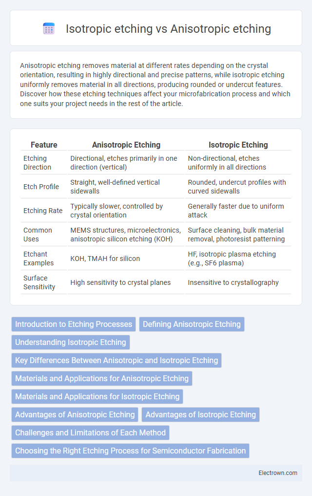
| Feature | Anisotropic Etching | Isotropic Etching |
|---|---|---|
| Etching Direction | Directional, etches primarily in one direction (vertical) | Non-directional, etches uniformly in all directions |
| Etch Profile | Straight, well-defined vertical sidewalls | Rounded, undercut profiles with curved sidewalls |
| Etching Rate | Typically slower, controlled by crystal orientation | Generally faster due to uniform attack |
| Common Uses | MEMS structures, microelectronics, anisotropic silicon etching (KOH) | Surface cleaning, bulk material removal, photoresist patterning |
| Etchant Examples | KOH, TMAH for silicon | HF, isotropic plasma etching (e.g., SF6 plasma) |
| Surface Sensitivity | High sensitivity to crystal planes | Insensitive to crystallography |
Introduction to Etching Processes
Etching processes in microfabrication involve selectively removing material from a substrate to create desired patterns. Anisotropic etching removes material at different rates depending on the crystal orientation, resulting in highly directional and precise features, whereas isotropic etching removes material uniformly in all directions, producing more rounded profiles. Your choice between anisotropic and isotropic etching impacts the resolution and profile of microstructures in semiconductor manufacturing.
Defining Anisotropic Etching
Anisotropic etching is a precise material removal process characterized by its directional etching properties, where etching rates differ based on crystal orientation or pattern geometry, enabling the creation of highly defined microstructures with vertical sidewalls. Unlike isotropic etching, which removes material uniformly in all directions and produces rounded features, anisotropic etching leverages reactant anisotropy or external factors such as crystallography to achieve sharp, rectangular profiles essential for semiconductor device fabrication and MEMS applications. This controlled etch behavior is critical in defining nanometer-scale features for integrated circuits and photonic components.
Understanding Isotropic Etching
Isotropic etching removes material uniformly in all directions, creating rounded or undercut profiles crucial for applications requiring smooth surface finishes. This etching method uses chemical solutions that react equally with the substrate, making it ideal for simple material removal without directional precision. Understanding isotropic etching is essential for selecting appropriate processes in microfabrication where shape control is less critical than uniform layer thinning.
Key Differences Between Anisotropic and Isotropic Etching
Anisotropic etching removes material at different rates depending on the crystallographic orientation, resulting in well-defined, directional profiles ideal for precise microfabrication. Isotropic etching, by contrast, etches uniformly in all directions, creating rounded or undercut features suitable for applications where directional control is less critical. Understanding these key differences helps you select the appropriate etching technique to achieve desired feature geometries and process outcomes in semiconductor manufacturing.
Materials and Applications for Anisotropic Etching
Anisotropic etching selectively removes material in specific directions, making it ideal for single-crystal silicon wafers in MEMS and microelectronics where precise geometries are critical. Common anisotropic etchants include potassium hydroxide (KOH) and tetramethylammonium hydroxide (TMAH), which exploit crystallographic orientations to create well-defined microstructures. This technique is essential for fabricating microfluidic channels, optical components, and integrated circuits requiring sharp, angular profiles.
Materials and Applications for Isotropic Etching
Isotropic etching uniformly removes material in all directions, making it suitable for etching materials like silicon dioxide, silicon nitride, and various polymers. This technique is often applied in MEMS fabrication, glass etching, and cleaning delicate surfaces where precise anisotropic profiles are not required. Understanding your material's compatibility with isotropic etching helps optimize processes in microelectronics and sensor manufacturing.
Advantages of Anisotropic Etching
Anisotropic etching offers superior precision in microfabrication by selectively etching materials along specific crystallographic planes, resulting in well-defined, vertical sidewalls. This method enhances dimensional accuracy and surface smoothness, crucial for semiconductor device performance and MEMS fabrication. When you require highly controlled etch profiles and minimal undercutting, anisotropic etching provides clear advantages over isotropic etching.
Advantages of Isotropic Etching
Isotropic etching offers uniform material removal in all directions, making it ideal for applications requiring smooth, rounded profiles and consistent etch depths. This process simplifies fabrication by reducing sensitivity to crystal orientation and enabling easier pattern transfer on diverse substrate materials. Its compatibility with a wide range of etchants and substrates enhances versatility in microfabrication and MEMS device production.
Challenges and Limitations of Each Method
Anisotropic etching faces challenges in achieving uniform etch rates across complex microstructures due to its directional dependence, which can result in uneven feature profiles and potential damage to delicate components. Isotropic etching, while simpler and more uniform in material removal, struggles with poor selectivity and loss of dimensional control, leading to undercutting and reduced precision in pattern transfer. Both methods are limited by trade-offs between etch rate, selectivity, and feature accuracy, impacting their suitability for advanced semiconductor manufacturing processes.
Choosing the Right Etching Process for Semiconductor Fabrication
Choosing the right etching process in semiconductor fabrication depends on the desired precision and feature geometry, with anisotropic etching providing directional control essential for creating well-defined, high-aspect-ratio structures, while isotropic etching offers uniform material removal suitable for smoothing and undercutting. Anisotropic etching utilizes reactive ion etching (RIE) or deep reactive ion etching (DRIE) techniques, delivering vertical sidewalls critical for advanced device architectures like FinFETs and MEMS. In contrast, isotropic etching, often achieved with wet chemical solutions, excels in bulk material removal but may compromise dimensional accuracy, influencing the selection based on specific fabrication requirements.
Anisotropic etching vs Isotropic etching Infographic