PCB vias and microvias both serve as electrical connections between layers on a printed circuit board, but microvias are significantly smaller and often laser-drilled to enable higher density and finer pitch designs. Understanding the differences in their construction, application, and performance can help you optimize your PCB design for advanced electronics. Explore the rest of this article to discover detailed insights on when to use each type.
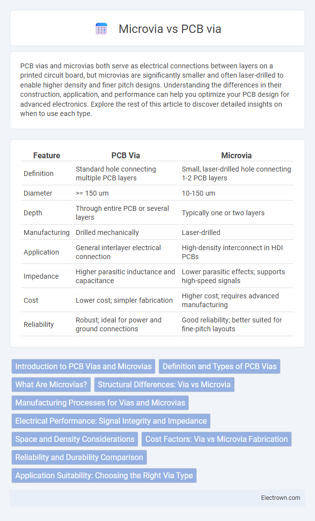
Table of Comparison
| Feature | PCB Via | Microvia |
|---|---|---|
| Definition | Standard hole connecting multiple PCB layers | Small, laser-drilled hole connecting 1-2 PCB layers |
| Diameter | >= 150 um | 10-150 um |
| Depth | Through entire PCB or several layers | Typically one or two layers |
| Manufacturing | Drilled mechanically | Laser-drilled |
| Application | General interlayer electrical connection | High-density interconnect in HDI PCBs |
| Impedance | Higher parasitic inductance and capacitance | Lower parasitic effects; supports high-speed signals |
| Cost | Lower cost; simpler fabrication | Higher cost; requires advanced manufacturing |
| Reliability | Robust; ideal for power and ground connections | Good reliability; better suited for fine-pitch layouts |
Introduction to PCB Vias and Microvias
PCB vias are essential conductive pathways that connect different layers within a printed circuit board, enabling electrical signals to pass vertically through the multi-layered structure. Microvias, significantly smaller than traditional vias with diameters typically less than 150 microns, offer improved signal integrity and higher circuit density, making them ideal for advanced high-frequency and high-density interconnect (HDI) designs. The selection between PCB vias and microvias depends on factors such as manufacturing capabilities, signal performance requirements, and board complexity.
Definition and Types of PCB Vias
PCB vias are conductive pathways that connect different layers in a printed circuit board, enabling electrical signals to travel vertically. Standard vias typically range from 150 to 500 microns in diameter, with through-hole vias passing through the entire board thickness, while blind and buried vias connect limited layers internally. Microvias, usually less than 150 microns in diameter, are laser-drilled and mainly used in HDI (High-Density Interconnect) boards to support miniaturization and high-speed signal integrity in compact designs.
What Are Microvias?
Microvias are tiny, laser-drilled holes in printed circuit boards (PCBs) that connect different layers within the board, typically measuring less than 150 microns in diameter. Unlike traditional vias, which can be several hundred microns wide, microvias offer higher density interconnections and are essential in advanced PCBs for mobile devices and high-frequency applications. Their small size reduces signal loss and crosstalk, improving electrical performance in multilayer PCB designs.
Structural Differences: Via vs Microvia
A standard PCB via is a drilled hole, typically ranging from 150 to 500 microns in diameter, that connects multiple layers of a printed circuit board electrically. Microvias are significantly smaller, usually less than 150 microns in diameter, created using laser drilling, and are limited to connecting adjacent layers only. Your PCB design's layer count and space constraints determine whether a via or microvia is the optimal choice for achieving reliable interlayer connections.
Manufacturing Processes for Vias and Microvias
PCB vias are manufactured through mechanical drilling or laser drilling, enabling the formation of holes that interconnect different layers, while microvias rely on precise laser drilling for creating smaller, high-density interconnections typically less than 150 microns in diameter. Microvia manufacturing requires advanced photolithography and plating techniques to achieve fine features and maintain signal integrity in high-frequency circuits. Your choice between vias and microvias depends on design complexity, layer count, and the precision required by modern high-density interconnect (HDI) PCBs.
Electrical Performance: Signal Integrity and Impedance
Microvias offer superior electrical performance compared to traditional PCB vias due to their smaller size, which reduces signal path length and minimizes parasitic inductance and capacitance, enhancing signal integrity. The reduced via diameter in microvias leads to lower impedance discontinuities, critical for high-frequency and high-speed digital signal applications. Optimizing via design with microvias ensures stable impedance control, minimizing signal reflections and losses in advanced PCB layouts.
Space and Density Considerations
Microvias offer significant space-saving advantages over traditional PCB vias by occupying a substantially smaller footprint, enabling higher component density and finer routing on printed circuit boards. Their reduced size and depth facilitate the creation of compact, multilayer PCBs with improved electrical performance and signal integrity in high-density applications. PCB designs demanding miniaturization and advanced functionality increasingly rely on microvias to optimize real estate and maximize circuit complexity without compromising reliability.
Cost Factors: Via vs Microvia Fabrication
Microvia fabrication generally incurs higher costs than traditional PCB vias due to advanced laser drilling technology and tighter manufacturing tolerances required for smaller diameters, typically below 150 microns. Material expenses also increase because microvias often need specialized dielectric layers and conductive plating to ensure reliability in high-density interconnects. While standard through-hole vias benefit from established mass production techniques and lower tooling costs, microvias are essential for compact, multilayer PCB designs where space optimization justifies the premium investment.
Reliability and Durability Comparison
Microvias exhibit higher reliability and durability in high-density PCB designs due to their smaller size, reducing thermal stress and the risk of cracking during thermal cycling. Traditional vias, while cost-effective for standard applications, are more prone to mechanical stress and conductor fatigue in multilayer boards with tight pitch requirements. Microvias also enhance signal integrity and reduce defect rates, prolonging PCB lifespan under rigorous operating conditions.
Application Suitability: Choosing the Right Via Type
PCB via selection depends on application suitability, with standard vias ideal for multi-layer boards needing robust electrical connections over longer distances. Microvias are optimal for high-density interconnects in compact devices, offering precise, space-saving pathways between adjacent layers. Understanding your design's signal integrity requirements and board complexity ensures the right via type enhances performance and reliability.
PCB via vs microvia Infographic