P-type semiconductors are created by adding elements with fewer electrons, resulting in positive charge carriers called holes, while n-type semiconductors are doped with elements that have extra electrons, providing negative charge carriers. Understanding the differences in their electrical properties and applications will help you grasp fundamental concepts in electronics; explore the rest of the article to deepen your knowledge.
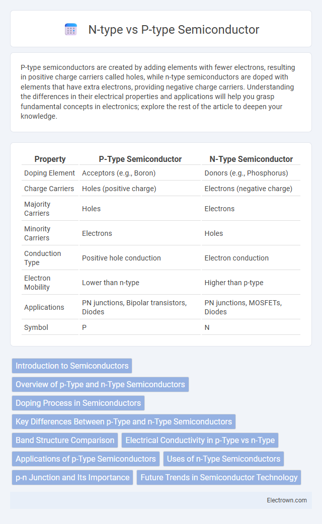
Table of Comparison
| Property | P-Type Semiconductor | N-Type Semiconductor |
|---|---|---|
| Doping Element | Acceptors (e.g., Boron) | Donors (e.g., Phosphorus) |
| Charge Carriers | Holes (positive charge) | Electrons (negative charge) |
| Majority Carriers | Holes | Electrons |
| Minority Carriers | Electrons | Holes |
| Conduction Type | Positive hole conduction | Electron conduction |
| Electron Mobility | Lower than n-type | Higher than p-type |
| Applications | PN junctions, Bipolar transistors, Diodes | PN junctions, MOSFETs, Diodes |
| Symbol | P | N |
Introduction to Semiconductors
P-type and n-type semiconductors are fundamental materials in modern electronics, distinguished by their charge carriers: holes in p-type and electrons in n-type. P-type semiconductors are created by doping silicon with elements like boron, which introduce positive charge carriers, while n-type semiconductors are doped with elements such as phosphorus, contributing extra electrons. These contrasting doping processes modify the electrical properties of semiconductors, enabling the formation of p-n junctions essential for diodes, transistors, and integrated circuits.
Overview of p-Type and n-Type Semiconductors
P-type semiconductors are created by doping a pure semiconductor, typically silicon, with elements like boron that have fewer valence electrons, resulting in the formation of "holes" which act as positive charge carriers. N-type semiconductors are formed by doping with elements such as phosphorus that have extra valence electrons, providing free electrons as negative charge carriers. Understanding your device's requirements helps determine whether p-type or n-type semiconductors best suit your electronic or photovoltaic applications due to their complementary electrical properties.
Doping Process in Semiconductors
The doping process in semiconductors involves introducing specific impurities to alter electrical conductivity, creating either p-type or n-type materials. P-type doping adds elements like boron with fewer valence electrons than silicon, generating positive "holes" that act as charge carriers. N-type doping introduces elements such as phosphorus with extra electrons, increasing the concentration of negative charge carriers and enhancing your device's performance by controlling charge flow.
Key Differences Between p-Type and n-Type Semiconductors
p-type semiconductors are created by doping a pure semiconductor with elements that provide an abundance of holes (positive charge carriers), whereas n-type semiconductors are doped with elements that add extra electrons (negative charge carriers). The majority charge carriers in p-type materials are holes, while in n-type materials they are electrons, affecting their electrical conductivity and behavior in electronic devices. Your choice between p-type and n-type semiconductors depends on their role in circuits, such as forming p-n junctions critical for diodes, transistors, and other semiconductor components.
Band Structure Comparison
P-type semiconductors have an abundance of holes as majority carriers created by acceptor impurities, causing the Fermi level to shift closer to the valence band. N-type semiconductors contain excess electrons as majority carriers due to donor impurities, which raises the Fermi level near the conduction band. Understanding the band structure difference between p-type and n-type materials is crucial for optimizing your semiconductor device performance.
Electrical Conductivity in p-Type vs n-Type
P-type semiconductors exhibit electrical conductivity primarily through the movement of positive holes created by the introduction of acceptor impurities, resulting in hole majority carriers. N-type semiconductors, on the other hand, conduct electricity mainly via free electrons introduced by donor impurities, making electrons the majority charge carriers. The conductivity in n-type materials generally surpasses that of p-type due to the higher mobility of electrons compared to holes.
Applications of p-Type Semiconductors
P-type semiconductors are widely used in electronic devices such as diodes, transistors, and solar cells due to their ability to create positive charge carriers (holes) that facilitate current flow. Their applications extend to complementary metal-oxide-semiconductor (CMOS) technology, where p-type materials form the essential components in p-channel MOSFETs, enhancing device efficiency. You rely on these semiconductors in power electronics and photodetectors, where controlled conductivity and charge carrier movement are critical for performance.
Uses of n-Type Semiconductors
N-type semiconductors, created by doping silicon with elements like phosphorus, are widely used in electronic devices to increase electron conductivity. These materials are essential in the fabrication of transistors, diodes, and integrated circuits, which form the backbone of modern electronics. Your devices rely on n-type semiconductors for efficient current flow and enhanced performance in applications such as solar cells and sensors.
p-n Junction and Its Importance
The p-n junction, formed by joining p-type and n-type semiconductors, is crucial for creating electronic devices like diodes and transistors due to its ability to control electron flow. In this junction, electrons from the n-type region combine with holes from the p-type region, generating a depletion region that acts as a barrier regulating current direction. Understanding this interaction enhances your ability to design efficient components for rectification, switching, and signal modulation.
Future Trends in Semiconductor Technology
Future trends in semiconductor technology emphasize advancements in p-type and n-type material engineering to enhance device performance and energy efficiency. Innovations in doping techniques aim to achieve higher carrier mobility and stability, crucial for next-generation transistors and integrated circuits. Research in two-dimensional semiconductors and heterojunctions leverages the unique properties of p-type and n-type layers to enable ultra-fast, low-power electronic and optoelectronic applications.
p-type vs n-type semiconductor Infographic