SEM provides detailed 3D surface images by scanning specimens with electrons, while TEM offers high-resolution 2D images revealing internal structures by transmitting electrons through thin samples. Discover how each technique suits your specific research needs by reading the full article.
Table of Comparison
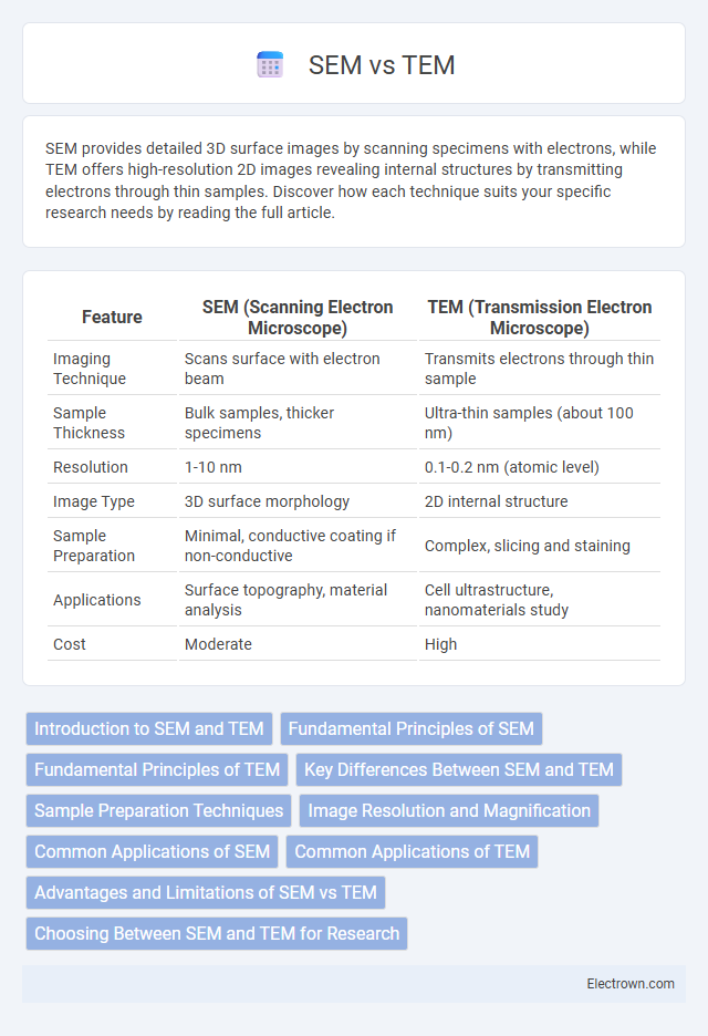
| Feature | SEM (Scanning Electron Microscope) | TEM (Transmission Electron Microscope) |
|---|---|---|
| Imaging Technique | Scans surface with electron beam | Transmits electrons through thin sample |
| Sample Thickness | Bulk samples, thicker specimens | Ultra-thin samples (about 100 nm) |
| Resolution | 1-10 nm | 0.1-0.2 nm (atomic level) |
| Image Type | 3D surface morphology | 2D internal structure |
| Sample Preparation | Minimal, conductive coating if non-conductive | Complex, slicing and staining |
| Applications | Surface topography, material analysis | Cell ultrastructure, nanomaterials study |
| Cost | Moderate | High |
Introduction to SEM and TEM
Scanning Electron Microscopy (SEM) uses focused electron beams to scan sample surfaces, generating detailed topographical images with high depth of field. Transmission Electron Microscopy (TEM) transmits electrons through ultra-thin specimens, offering atomic-scale resolution to examine internal structures. Understanding the differences in imaging techniques helps optimize your choice for material analysis or biological research.
Fundamental Principles of SEM
Scanning Electron Microscopy (SEM) operates by directing a focused beam of electrons onto a specimen's surface, causing the emission of secondary electrons that produce high-resolution, three-dimensional images. The fundamental principle relies on detecting these emitted electrons to reveal surface topography and composition at nanoscale detail. Understanding SEM's electron-sample interactions allows you to analyze surface morphology with exceptional depth of field and spatial resolution compared to Transmission Electron Microscopy (TEM).
Fundamental Principles of TEM
Transmission Electron Microscopy (TEM) operates by transmitting a high-energy electron beam through an ultra-thin specimen, allowing for imaging at atomic resolution. Unlike Scanning Electron Microscopy (SEM), which scans the surface, TEM's fundamental principle relies on electron scattering and interaction within the sample, producing detailed internal structural information. Your analysis benefits from TEM's capacity to reveal crystallographic, morphological, and compositional details at the nanoscale level.
Key Differences Between SEM and TEM
Scanning Electron Microscopy (SEM) provides detailed 3D surface morphology by scanning the specimen with a focused electron beam, while Transmission Electron Microscopy (TEM) offers high-resolution 2D internal structure imaging by transmitting electrons through ultra-thin samples. SEM typically achieves resolution around 1-20 nanometers, ideal for topographical analysis, whereas TEM attains sub-nanometer resolution, enabling atomic-scale visualization. Sample preparation for SEM is less complex compared to TEM, which requires extensive thinning and electron transparency for accurate internal imaging.
Sample Preparation Techniques
SEM sample preparation typically involves coating specimens with a thin layer of conductive material like gold or carbon to prevent charging and enhance image quality, requiring minimal alteration of surface morphology. TEM sample preparation is more complex, demanding ultra-thin sections (usually less than 100 nanometers) achieved through microtomy or ion milling to allow electron transmission through the specimen. Your expertise in selecting appropriate preparation techniques directly influences imaging resolution and accuracy for either Scanning Electron Microscopy or Transmission Electron Microscopy.
Image Resolution and Magnification
Scanning Electron Microscopes (SEM) typically offer image resolutions ranging from 1 to 20 nanometers with magnifications up to around 500,000x, ideal for detailed surface imaging. Transmission Electron Microscopes (TEM) provide superior resolution down to 0.1 nanometers and magnifications exceeding 1,000,000x, enabling visualization of internal structures at the atomic level. The higher resolution and magnification capabilities of TEM make it essential for applications requiring atomic-scale imaging, while SEM remains preferred for three-dimensional surface topography.
Common Applications of SEM
Scanning Electron Microscopy (SEM) is commonly used for detailed surface morphology analysis in materials science, semiconductor inspection, and biological specimen imaging. SEM's ability to provide high-resolution, three-dimensional images makes it ideal for failure analysis and quality control in industrial processes. The technique is also widely employed in forensic science for particle characterization and trace evidence examination.
Common Applications of TEM
Transmission Electron Microscopy (TEM) excels in high-resolution imaging, making it indispensable for analyzing nanoscale structures, including crystalline defects, atomic arrangements, and thin film compositions in materials science. It is widely used in biology to visualize subcellular organelles, viruses, and macromolecular complexes at the molecular level. TEM also plays a crucial role in semiconductor research and development by enabling detailed inspection of microelectronic device structures and interfaces.
Advantages and Limitations of SEM vs TEM
Scanning Electron Microscopy (SEM) provides detailed three-dimensional images of sample surfaces with high depth of field, making it ideal for studying surface morphology and texture, while Transmission Electron Microscopy (TEM) offers superior resolution at the atomic or molecular level, enabling visualization of internal structures and crystallography. SEM is generally faster, more versatile, and requires simpler sample preparation, but its resolution is limited to around 1-10 nanometers, whereas TEM demands ultra-thin samples and complex preparation, limiting its use to very small or specially prepared specimens. Your choice between SEM and TEM should consider whether surface detail or internal ultrastructure analysis is the priority, alongside practical constraints like sample preparation and resolution needs.
Choosing Between SEM and TEM for Research
Choosing between SEM (Scanning Electron Microscopy) and TEM (Transmission Electron Microscopy) depends on the research requirements for resolution and sample analysis. SEM offers surface imaging with high depth of field ideal for 3D morphology, while TEM provides ultra-high resolution for detailed internal structures at the atomic or molecular level. Your decision should be guided by whether surface topology or internal composition analysis is the primary focus of your study.
SEM vs TEM Infographic